鈥?/div>
16
SOIC鈭?6
D SUFFIX
CASE 751B
1
140xxB
AWLYWW
High Source and Sink Currents
High鈭抰o鈭扡ow Level Converter
Supply Voltage Range = 3.0 V to 18 V
V
IN
can exceed V
DD
Meets JEDEC B Specifications
Improved ESD Protection On All Inputs
Pb鈭扚ree Packages are Available*
16
TSSOP鈭?6
DT SUFFIX
CASE 948F
1
Value
鈭?.5 to +18.0
鈭?.5 to +18.0
鈭?.5 to V
DD
+
0.5
卤
10
卤
45
825
740
鈭?5 to +125
鈭?5 to +150
260
掳C
掳C
掳C
Unit
V
V
V
mA
mA
mW
xx
A
WL, L
YY, Y
WW, W
= Specific Device Code
= Assembly Location
= Wafer Lot
= Year
= Work Week
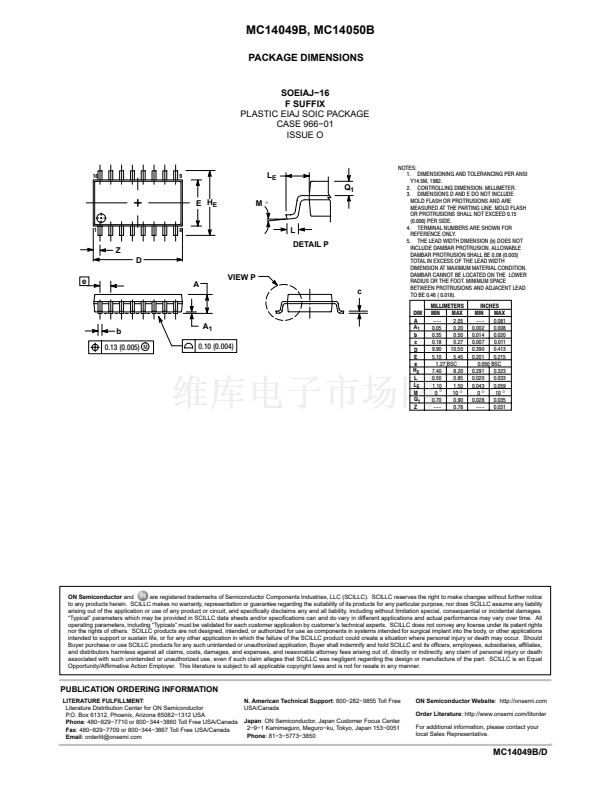
SOEIAJ鈭?6
F SUFFIX
CASE 966
1
16
MC140xxB
AWLYWW
14
0xxB
ALYW
MAXIMUM RATINGS
(Voltages Referenced to V
SS
)
Symbol
V
DD
V
in
V
out
I
in
I
out
P
D
Parameter
DC Supply Voltage Range
Input Voltage Range (DC or Transient)
Output Voltage Range (DC or Transient)
Input Current (DC or Transient) per Pin
Output Current (DC or Transient) per Pin
Power Dissipation, per Package (Note 1)
(Plastic)
(SOIC)
Ambient Temperature Range
Storage Temperature Range
Lead Temperature (8鈭扴econd Soldering)
T
A
T
stg
T
L
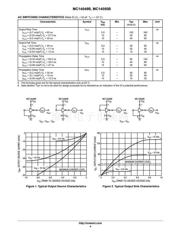
1. Temperature Derating: See Figure 3.
This device contains protection circuitry to protect the inputs against damage
due to high static voltages or electric fields referenced to the V
SS
pin only. Extra
precautions must be taken to avoid applications of any voltage higher than the
maximum rated voltages to this high鈭抜mpedance circuit. For proper operation, the
ranges V
SS
鈮?/div>
V
in
鈮?/div>
18 V and V
SS
鈮?/div>
V
out
鈮?/div>
V
DD
are recommended.
Unused inputs must always be tied to an appropriate logic voltage level
(e.g., either V
SS
or V
DD
). Unused outputs must be left open.
ORDERING INFORMATION
See detailed ordering and shipping information in the package
dimensions section on page 2 of this data sheet.
*For additional information on our Pb鈭扚ree strategy and soldering details, please
download the ON Semiconductor Soldering and Mounting Techniques
Reference Manual, SOLDERRM/D.
漏
Semiconductor Components Industries, LLC, 2005
1
February, 2005 鈭?Rev. 5
Publication Order Number:
MC14049B/D


 1
1
 2
2
 3
3
 4
4
 5
5
 6
6
 7
7
 8
8
