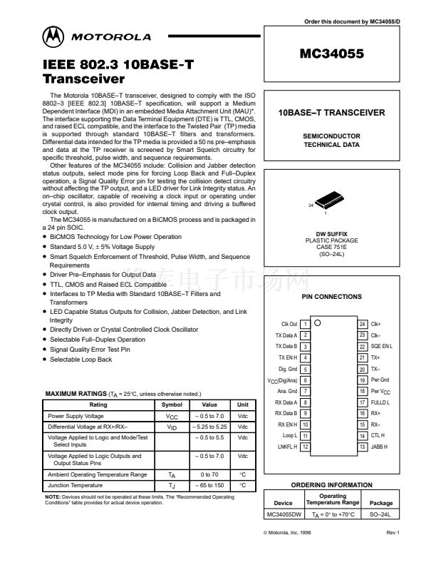
Order this document by MC34055/D
IEEE 802.3 10BASE-T
Transceiver
The Motorola 10BASE鈥揟 transceiver, designed to comply with the ISO
8802鈥? [IEEE 802.3] 10BASE鈥揟 specification, will support a Medium
Dependent Interface (MDI) in an embedded Media Attachment Unit (MAU)*.
The interface supporting the Data Terminal Equipment (DTE) is TTL, CMOS,
and raised ECL compatible, and the interface to the Twisted Pair (TP) media
is supported through standard 10BASE鈥揟 filters and transformers.
Differential data intended for the TP media is provided a 50 ns pre鈥揺mphasis
and data at the TP receiver is screened by Smart Squelch circuitry for
specific threshold, pulse width, and sequence requirements.
Other features of the MC34055 include: Collision and Jabber detection
status outputs, select mode pins for forcing Loop Back and Full鈥揇uplex
operation, a Signal Quality Error pin for testing the collision detect circuitry
without affecting the TP output, and a LED driver for Link Integrity status. An
on鈥揷hip oscillator, capable of receiving a clock input or operating under
crystal control, is also provided for internal timing and driving a buffered
clock output.
The MC34055 is manufactured on a BiCMOS process and is packaged in
a 24 pin SOIC.
鈥?/div>
BiCMOS Technology for Low Power Operation
MC34055
10BASE鈥揟 TRANSCEIVER
SEMICONDUCTOR
TECHNICAL DATA
24
1
鈥?/div>
鈥?/div>
鈥?/div>
鈥?/div>
鈥?/div>
鈥?/div>
鈥?/div>
鈥?/div>
鈥?/div>
鈥?/div>
Standard 5.0 V,
卤
5% Voltage Supply
Smart Squelch Enforcement of Threshold, Pulse Width, and Sequence
Requirements
Driver Pre鈥揈mphasis for Output Data
TTL, CMOS and Raised ECL Compatible
Interfaces to TP Media with Standard 10BASE鈥揟 Filters and
Transformers
LED Capable Status Outputs for Collision, Jabber Detection, and Link
Integrity
Directly Driven or Crystal Controlled Clock Oscillator
Selectable Full鈥揇uplex Operation
Signal Quality Error Test Pin
Selectable Loop Back
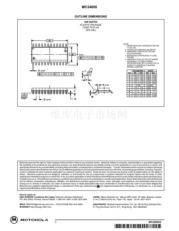
DW SUFFIX
PLASTIC PACKAGE
CASE 751E
(SO鈥?4L)
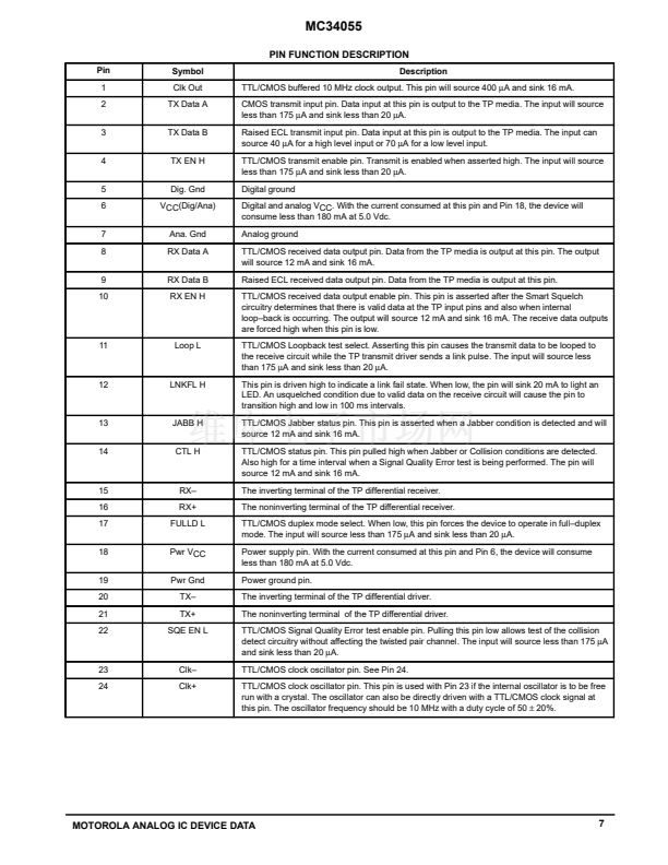
PIN CONNECTIONS
Clk Out
TX Data A
TX Data B
TX EN H
Dig. Gnd
VCC(Dig/Ana)
1
2
3
4
5
6
7
8
9
24
23
22
21
20
19
18
17
16
15
14
13
Clk+
Clk鈥?/div>
SQE EN L
TX+
TX鈥?/div>
Pwr Gnd
Pwr VCC
FULLD L
RX+
RX鈥?/div>
CTL H
JABB H
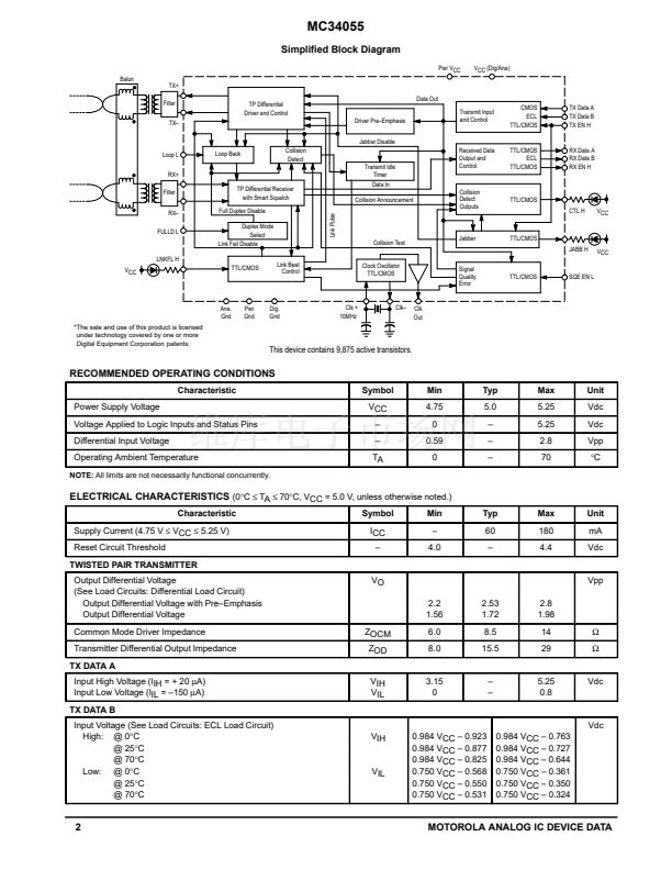
MAXIMUM RATINGS
(TA = 25掳C, unless otherwise noted.)
Rating
Power Supply Voltage
Differential Voltage at RX+/RX鈥?/div>
Voltage Applied to Logic and Mode/Test
Select Inputs
Voltage Applied to Logic Outputs and
Output Status Pins
Ambient Operating Temperature Range
Junction Temperature
TA
TJ
Symbol
VCC
VID
Value
鈥?0.5 to 7.0
鈥?5.25 to 5.25
鈥?0.5 to 5.5
鈥?0.5 to 7.0
0 to 70
鈥?65 to 150
Unit
Vdc
Vdc
Vdc
Vdc
掳C
掳C
Ana. Gnd
RX Data A
RX Data B
RX EN H 10
Loop L
11
LNKFL H 12
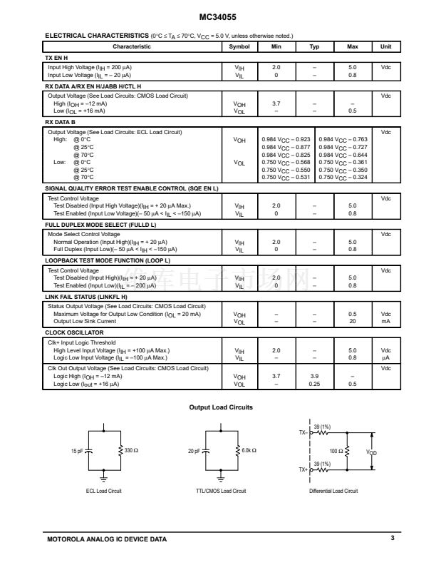
ORDERING INFORMATION
Device
MC34055DW
漏
Motorola, Inc. 1996
NOTE:
Devices should not be operated at these limits. The 鈥淩ecommended Operating
Conditions鈥?table provides for actual device operation.
Operating
Temperature Range
TA = 0掳 to +70掳C
Package
SO鈥?4L
Rev 1
MOTOROLA ANALOG IC DEVICE DATA
1
MC34055DW相关型号PDF文件下载
-
型号
版本
描述
厂商
下载
-
英文版
Motorola, Inc [QUAD SINGLE SUPPLY OPERATIONAL AMPLIFIERS]
-
英文版
飞思卡尔
-
英文版
飞思卡尔
-
英文版
QUADRUPLE LOW-POWER OPERATIONAL AMPLIFIERS
-
英文版
QUAD DIFFERENTIAL INPUT OPERATIONAL AMPLIFIERS
-
英文版
LOW POWER QUAD BIPOLAR OPERATIONAL AMPLIFIERS
STMicro
-
英文版
DUAL OPERATIONAL AMPLIFIER / DUAL VOLTAGE COMPARATOR
ONSEMI
-
英文版
飞思卡尔
-
英文版
DUAL OPERATIONAL AMPLIFIER / DUAL VOLTAGE COMPARATOR
-
英文版
飞思卡尔
-
英文版
飞思卡尔
-
英文版
10-Bit high-speed multiplying D/A converter
PHILIPS
-
英文版
10-Bit high-speed multiplying D/A converter
PHILIPS [P...
-
英文版
飞思卡尔
-
英文版
飞思卡尔
-
英文版
飞思卡尔
-
英文版
飞思卡尔
-
英文版
飞思卡尔
-
英文版
飞思卡尔
-
英文版
Unisonic Technologies [LOW POWER AUDIO AMPLIFIER]
UTC


 1
1
 2
2
 3
3
 4
4
 5
5
 6
6
 7
7
 8
8
 9
9
 10
10
 11
11
 12
12
 13
13
 14
14
 15
15
 16
16
