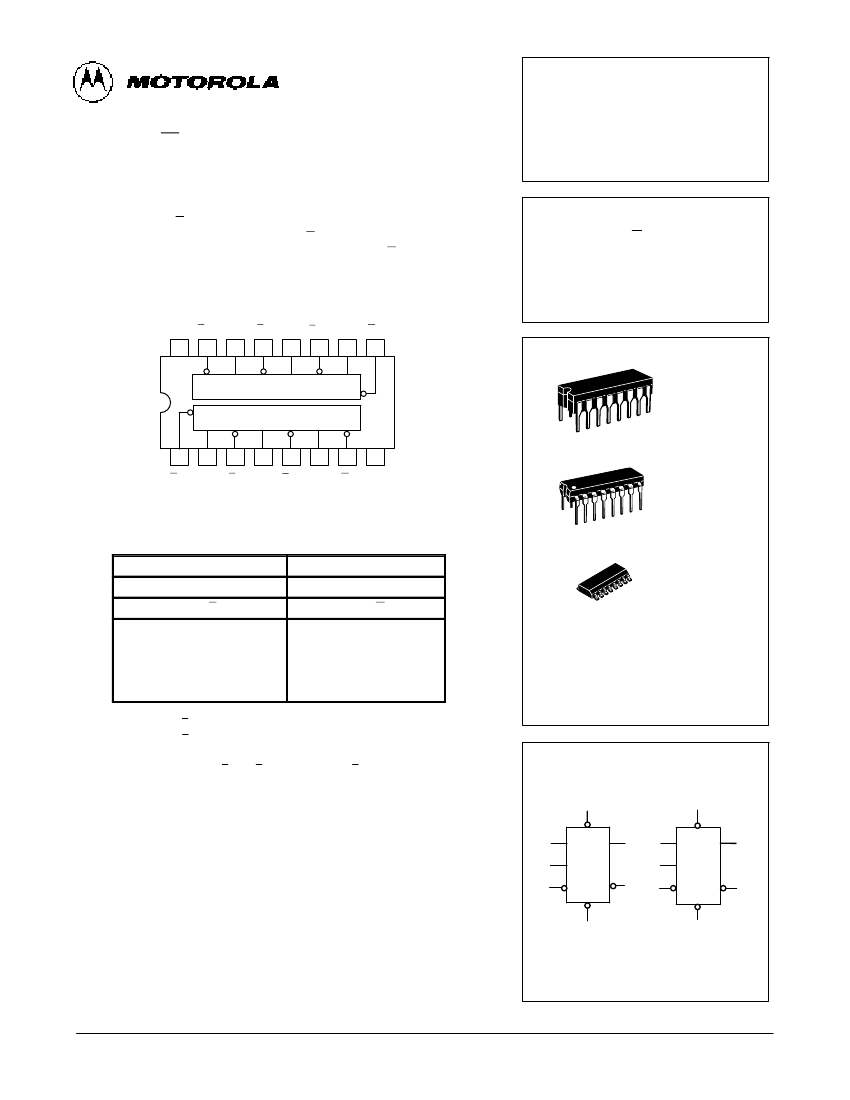
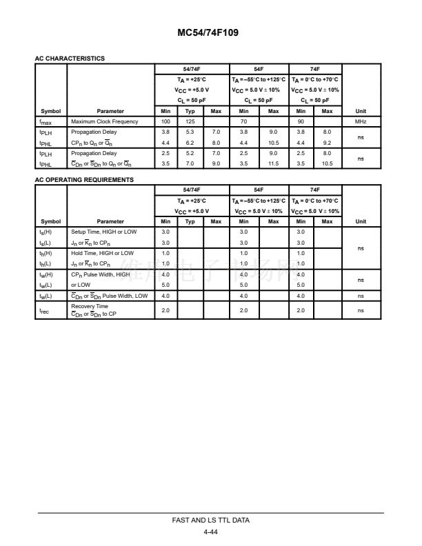
MC54/74F109
DUAL JK POSITIVE
EDGE-TRIGGERED FLIP-FLOP
The MC54/74F109 consists of two high-speed, completely independent
transition clocked JK flip-flops. The clocking operation is independent of rise
and fall times of the clock waveform. The JK design allows operation as a D
flip-flop (refer to F74 data sheet) by connecting the J and K inputs together.
DUAL JK POSITIVE
EDGE-TRIGGERED FLIP-FLOP
FAST鈩?SCHOTTKY TTL
CONNECTION DIAGRAM
VCC CD2
16
15
CD
CD1
J1
1
CD1
2
J1
J2
14
J
K2
13
K
CP2 SD2
11
12
CP
SD
Q2
10
Q
Q
Q1
7
Q1
8
GND
16
1
16
1
Q2
9
K1
3
K1
CP1 SD1
4
5
Q1
6
Q1
J SUFFIX
CERAMIC
CASE 620-09
CP1 SD1
N SUFFIX
PLASTIC
CASE 648-08
FUNCTION TABLE (Each Half)
Input
@ tn
J
L
L
H
H
Asynchronous Inputs:
LOW Input to SD sets Q to HIGH level
LOW Input to CD sets Q to LOW level
Clear and Set are independent of clock
Simultaneous LOW on CD and SD makes both Q and Q HIGH
H = HIGH Voltage Level
L = LOW Voltage Level
tn = Bit time before clock pulse
tn + 1 = Bit time after clock pulse
Output
@ tn + 1
Q
Q
16
1
K
H
L
H
L
D SUFFIX
SOIC
CASE 751B-03
No Change
L
H
H
L
ORDERING INFORMATION
MC54FXXXJ
MC74FXXXN
MC74FXXXD
Ceramic
Plastic
SOIC
Toggles
LOGIC SYMBOL
5
2
4
3
J
SD
Q
J
11
SD
Q
6
14
12
10
CP
K C Q
D
1
7
CP
K
CD
15
Q
9
13
VCC = PIN 16
GND = PIN 8
FAST AND LS TTL DATA
4-42


 1
1
 2
2
 3
3
