鈥?/div>
Pb鈭扚ree Package is Available
MAXIMUM RATINGS
http://onsemi.com
Rating
Symbol
V
CEO
V
CER
V
CB
V
EB
I
C
I
B
Value
60
70
Unit
Vdc
Vdc
Vdc
Vdc
Adc
Adc
Collector鈭扙mitter Voltage
15 A
POWER TRANSISTORS
COMPLEMENTARY SILICON
60 V
115 W
MARKING
DIAGRAM
PD, POWER DISSIPATION (WATTS)
脦脦脦脦脦脦脦脦脦脦脦脦脦脦脦脦脦脦脦
脦 脦 脦
脦脦脦脦脦脦脦脦脦脦脦脦脦脦脦脦脦脦脦
脦脦 脦 脦
脦
脦脦脦脦脦脦脦脦脦脦脦脦脦脦脦脦脦脦脦
脦 脦 脦
脦脦脦脦脦脦脦脦脦脦脦脦脦脦脦脦脦脦脦
脦 脦 脦
脦
脦 脦
脦脦脦脦脦脦脦脦脦脦脦脦脦脦脦脦脦脦脦
脦
脦脦脦脦脦脦脦脦脦脦脦脦脦脦脦脦脦脦脦
脦
脦 脦
脦脦 脦 脦
脦脦脦脦脦脦脦脦脦脦脦脦脦脦脦脦脦脦脦
脦脦脦脦脦脦脦脦脦脦脦脦脦脦脦脦脦脦
脦 脦 脦
脦脦脦脦脦脦脦脦脦脦脦脦脦脦脦脦脦脦脦
脦脦 脦 脦
脦脦脦脦脦脦脦脦脦脦脦脦脦脦脦脦脦脦脦
脦 脦 脦
脦脦脦脦脦脦脦脦脦脦脦脦脦脦脦脦脦脦脦
脦 脦 脦
脦脦脦脦脦脦脦脦脦脦脦脦脦脦脦脦脦脦脦
脦 脦 脦
脦脦脦脦脦脦脦脦脦脦脦脦脦脦脦脦脦脦脦
脦 脦 脦
脦脦脦脦脦脦脦脦脦脦脦脦脦脦脦脦脦脦脦
脦 脦 脦
脦 脦 脦
脦 脦
脦脦脦脦脦脦脦脦脦脦脦脦脦脦脦脦脦脦脦
脦 脦 脦
脦脦脦脦脦脦脦脦脦脦脦脦脦脦脦脦脦脦脦
脦脦脦脦脦脦脦脦脦脦脦脦脦脦脦脦脦脦
脦
脦脦脦脦脦脦脦脦脦脦脦脦脦脦脦脦脦脦脦
脦 脦 脦
脦脦 脦 脦
脦 脦 脦
脦脦脦脦脦脦脦脦脦脦脦脦脦脦脦脦脦脦脦
脦 脦 脦
脦脦脦脦脦脦脦脦脦脦脦脦脦脦脦脦脦脦脦
脦 脦 脦
脦脦脦脦脦脦脦脦脦脦脦脦脦脦脦脦脦脦脦
脦脦脦脦脦脦脦脦脦脦脦脦脦脦脦脦脦脦
脦脦脦脦脦脦脦脦脦脦脦脦脦脦脦脦脦脦脦
脦 脦 脦
脦 脦
脦脦脦脦脦脦脦脦脦脦脦脦脦脦脦脦脦脦脦
脦脦脦脦脦脦脦脦脦脦脦脦脦脦脦脦脦脦
脦 脦
Collector鈭扙mitter Voltage
Collector鈭払ase Voltage
Emitter鈭払ase Voltage
100
7
Collector Current 鈭?Continuous
Base Current
15
7
Total Power Dissipation @ T
C
= 25掳C
Derate above 25掳C
P
D
115
0.657
W
W/掳C
掳C
Operating and Storage Junction Tempera-
ture Range
T
J
, T
stg
鈥?65 to + 200
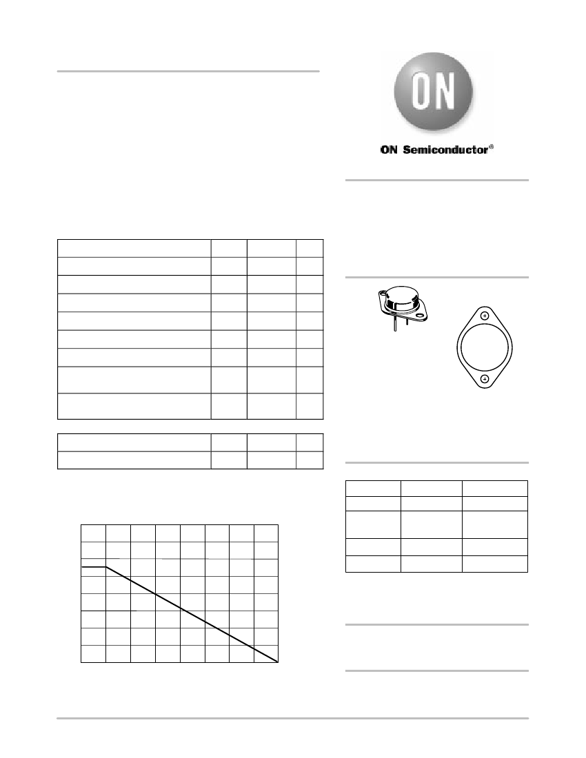
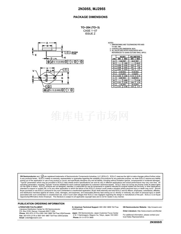
TO鈭?04AA (TO鈭?)
CASE 1鈭?7
xxxx55
A
YYWW
THERMAL CHARACTERISTICS
Characteristic
Symbol
R
qJC
Max
Unit
xxxx55 = Device Code
xxxx= 2N3055 or MJ2955
A
= Assembly Location
YY
= Year
WW = Work Week
x
= 1, 2, or 3
Thermal Resistance, Junction鈭抰o鈭扖ase
1.52
掳C/W
Maximum ratings are those values beyond which device damage can occur.
Maximum ratings applied to the device are individual stress limit values (not
normal operating conditions) and are not valid simultaneously. If these limits
are exceeded, device functional operation is not implied, damage may occur
and reliability may be affected.
160
140
120
100
80
60
40
20
0
0
25
50
75
100
125
150
175
200
ORDERING INFORMATION
Device
2N3055
2N3055G
Package
TO鈭?04AA
TO鈭?04AA
(Pb鈭扚ree)
TO鈭?04AA
TO鈭?04AA
Shipping
鈥?/div>
100 Units / Tray
1 Units / Tubes
2N3055H
MJ2955
100 Units / Tray
100 Units / Tray
鈥燜or information on tape and reel specifications,
including part orientation and tape sizes, please
refer to our Tape and Reel Packaging Specifications
Brochure, BRD8011/D.
*For additional information on our Pb鈭扚ree strategy
and soldering details, please download the
ON Semiconductor Soldering and Mounting
Techniques Reference Manual, SOLDERRM/D.
T
C
, CASE TEMPERATURE (掳C)
Preferred
devices are recommended choices for future use
and best overall value.
Figure 1. Power Derating
漏
Semiconductor Components Industries, LLC, 2004
1
April, 2004 鈭?Rev. 4
Publication Order Number:
2N3055/D


 1
1
 2
2
 3
3
 4
4
