鈥?/div>
Electrically Similar to Popular TIP31 and TIP32 Series
MAXIMUM RATINGS
Rating
Collector鈭扙mitter Voltage
Collector鈭払ase Voltage
Emitter鈭払ase Voltage
Collector Current 鈭?Continuous
Peak
Base Current
Total Power Dissipation @ T
C
= 25掳C
Derate above 25掳C
Total Power Dissipation* @ T
A
= 25掳C
Derate above 25掳C
Operating and Storage Junction Temperature
Range
Symbol
V
CEO
V
CB
V
EB
I
C
I
B
P
D
P
D
T
J
, T
stg
Max
100
100
5
2
4
50
20
0.16
1.75
0.014
鈭?5 to
+ 150
Unit
Vdc
Vdc
Vdc
Adc
1
2
mAdc
W
W/掳C
W
W/掳C
掳C
3
1 2
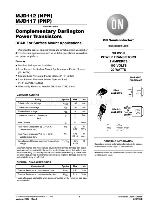
SILICON
POWER TRANSISTORS
2 AMPERES
100 VOLTS
20 WATTS
MARKING
DIAGRAMS
4
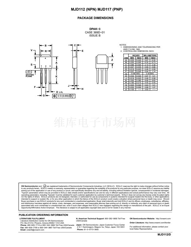
DPAK
CASE 369C
3
YWW
J11x
4
DPAK鈭?
CASE 369D
YWW
J11x
Y
WW
x
= Year
= Work Week
= 2 or 7
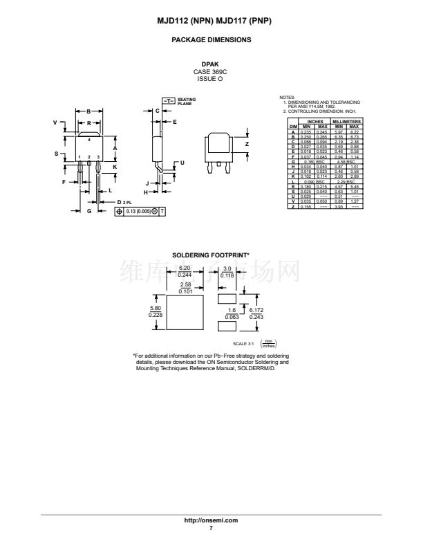
ORDERING INFORMATION
See detailed ordering and shipping information in the package
dimensions section on page 2 of this data sheet.
Preferred
devices are recommended choices for future use
and best overall value.
Maximum ratings are those values beyond which device damage can occur.
Maximum ratings applied to the device are individual stress limit values (not
normal operating conditions) and are not valid simultaneously. If these limits
are exceeded, device functional operation is not implied, damage may occur
and reliability may be affected.
THERMAL CHARACTERISTICS
Characteristic
Thermal Resistance, Junction鈭抰o鈭扖ase
Thermal Resistance, Junction鈭抰o鈭扐mbient*
Symbol
R
qJC
R
qJA
Max
6.25
71.4
Unit
掳C/W
掳C/W
*These ratings are applicable when surface mounted on the minimum pad sizes
recommended.
漏
Semiconductor Components Industries, LLC, 2004
1
August, 2004 鈭?Rev. 5
Publication Order Number:
MJD112/D


 1
1
 2
2
 3
3
 4
4
 5
5
 6
6
 7
7
 8
8
