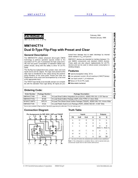
MM74HCT74 Dual D-Type Flip-Flop with Preset and Clear
February 1984
Revised January 1999
MM74HCT74
Dual D-Type Flip-Flop with Preset and Clear
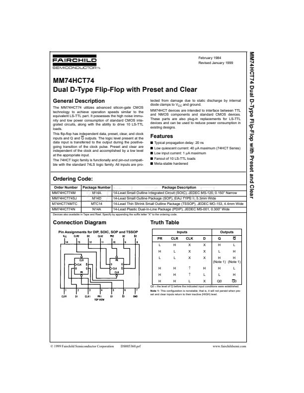
General Description
The MM74HCT74 utilizes advanced silicon-gate CMOS
technology to achieve operation speeds similar to the
equivalent LS-TTL part. It possesses the high noise immu-
nity and low power consumption of standard CMOS inte-
grated circuits, along with the ability to drive 10 LS-TTL
loads.
This flip-flop has independent data, preset, clear, and clock
inputs and Q and Q outputs. The logic level present at the
data input is transferred to the output during the positive-
going transition of the clock pulse. Preset and clear are
independent of the clock and accomplished by a low level
at the appropriate input.
The 74HCT logic family is functionally and pin-out compati-
ble with the standard 74LS logic family. All inputs are pro-
tected from damage due to static discharge by internal
diode clamps to V
CC
and ground.
MM74HCT devices are intended to interface between TTL
and NMOS components and standard CMOS devices.
These parts are also plug-in replacements for LS-TTL
devices and can be used to reduce power consumption in
existing designs.
Features
s
Typical propagation delay: 20 ns
s
Low quiescent current: 40
碌A
maximum (74HCT Series)
s
Low input current: 1
碌A
maximum
s
Fanout of 10 LS-TTL loads
s
Meta-stable hardened
Ordering Code:
Order Number
MM74HCT74M
MM74HCT74SJ
M74HCT74MTC
MM74HCT74N
Package Number
M14A
M14D
MTC14
N14A
Package Description
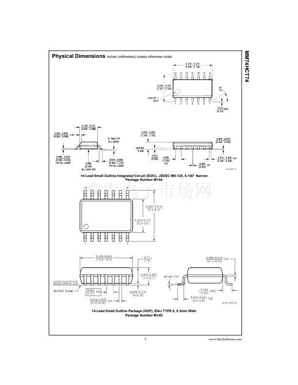
14-Lead Small Outline Integrated Circuit (SOIC), JEDEC MS-120, 0.150鈥?Narrow
14-Lead Small Outline Package (SOP), EIAJ TYPE II, 5.3mm Wide
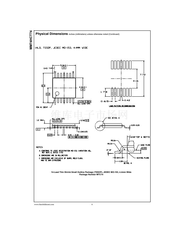
14-Lead Thin Shrink Small Outline Package (TSSOP), JEDEC MO-153, 4.4mm Wide
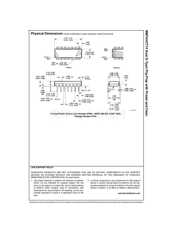
14-Lead Plastic Dual-In-Line Package (PDIP), JEDEC MS-001, 0.300鈥?Wide
Devices also available in Tape and Reel. Specify by appending the suffix letter 鈥淴鈥?to the ordering code.
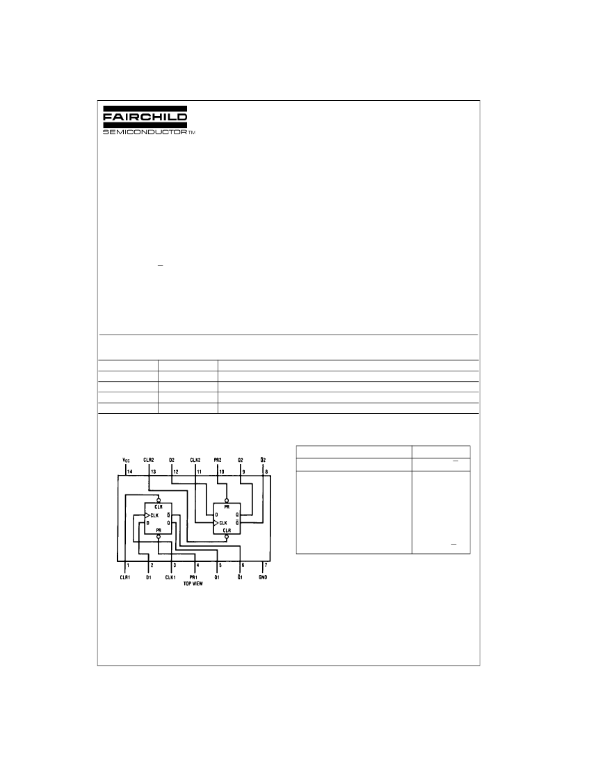
Connection Diagram
Pin Assignments for DIP, SOIC, SOP and TSSOP
Truth Table
Inputs
PR
L
H
L
H
H
H
CLR
H
L
L
H
H
H
CLK
X
X
X
鈫?/div>
鈫?/div>
L
D
X
X
X
H
L
X
Outputs
Q
H
L
Q
L
H
H
H
(Note 1) (Note 1)
H
L
Q0
L
H
Q0
Q0
=
the level of Q before the indicated input conditions were established.
Note 1:
This configuration is nonstable; that is, it will not persist when pre-
set and clear inputs return to their inactive (HIGH) level.
漏 1999 Fairchild Semiconductor Corporation
DS005360.prf
www.fairchildsemi.com


 1
1
 2
2
 3
3
 4
4
 5
5
 6
6
 7
7
