鈥?/div>
Pb鈭扚ree Packages are Available
MAXIMUM RATINGS
Rating
Collector 鈭扙mitter Voltage
Collector 鈭払ase Voltage
Emitter 鈭払ase Voltage
Collector Current 鈭?Continuous
Symbol
V
CEO
V
CBO
V
EBO
I
C
Value
鈭?0
鈭?0
鈭?.0
鈭?00
Unit
Vdc
Vdc
Vdc
mAdc
http://onsemi.com
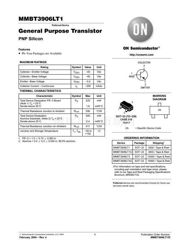
COLLECTOR
3
1
BASE
2
EMITTER
THERMAL CHARACTERISTICS
Characteristic
Total Device Dissipation FR鈭?5 Board
(Note 1) T
A
= 25掳C
Derate above 25掳C
Thermal Resistance Junction to Ambient
Total Device Dissipation
Alumina Substrate, (Note 2) T
A
= 25掳C
Derate above 25掳C
Thermal Resistance Junction鈭抰o鈭扐mbient
Junction and Storage Temperature
Symbol
P
D
Max
225
1.8
R
qJA
P
D
556
300
2.4
R
qJA
T
J
, T
stg
417
鈭?5 to
+150
Unit
mW
mW/掳C
掳C/W
mW
mW/掳C
掳C/W
掳C
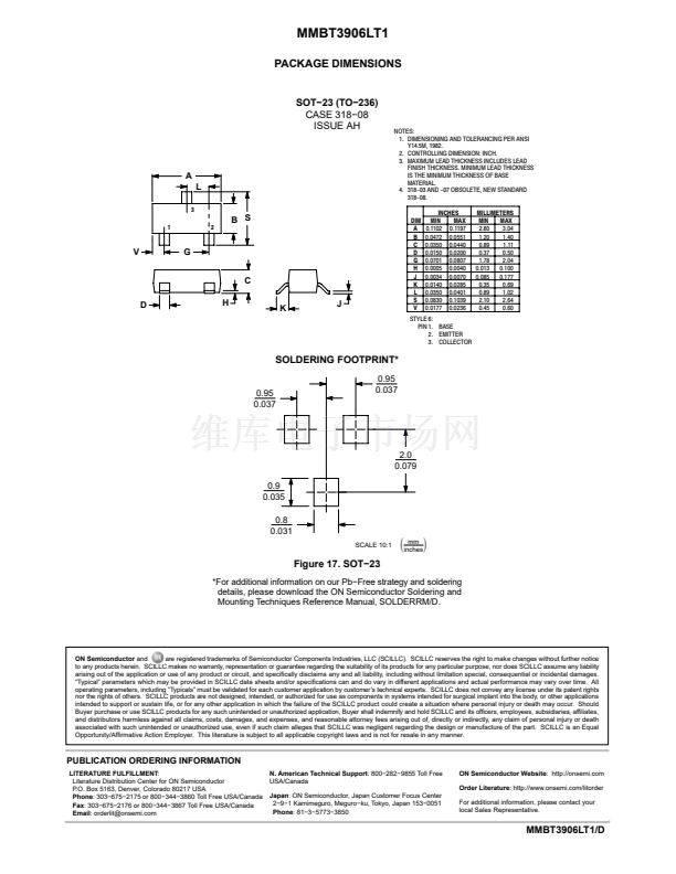
1
2
SOT鈭?3 (TO鈭?36)
CASE 318
Style 6
2A
= Specific Device Code
2A
3
MARKING
DIAGRAM
1. FR鈭? = 1.0
�
0.75
�
0.062 in.
2. Alumina = 0.4
�
0.3
�
0.024 in. 99.5% alumina.
ORDERING INFORMATION
Device
MMBT3906LT1
MMBT3906LT1G
MMBT3906LT3
MMBT3906LT3G
Package
SOT鈭?3
SOT鈭?3
SOT鈭?3
SOT鈭?3
Shipping
鈥?/div>
3000 / Tape & Reel
3000 / Tape & Reel
10000 / Tape & Reel
10000 / Tape & Reel
鈥燜or information on tape and reel specifications,
including part orientation and tape sizes, please
refer to our Tape and Reel Packaging Specifications
Brochure, BRD8011/D.
Preferred
devices are recommended choices for future use
and best overall value.
漏
Semiconductor Components Industries, LLC, 2004
1
February, 2004 鈭?Rev. 4
Publication Order Number:
MMBT3906LT1/D


 1
1
 2
2
 3
3
 4
4
 5
5
 6
6
