鈥?/div>
Pb鈭扚ree Package is Available
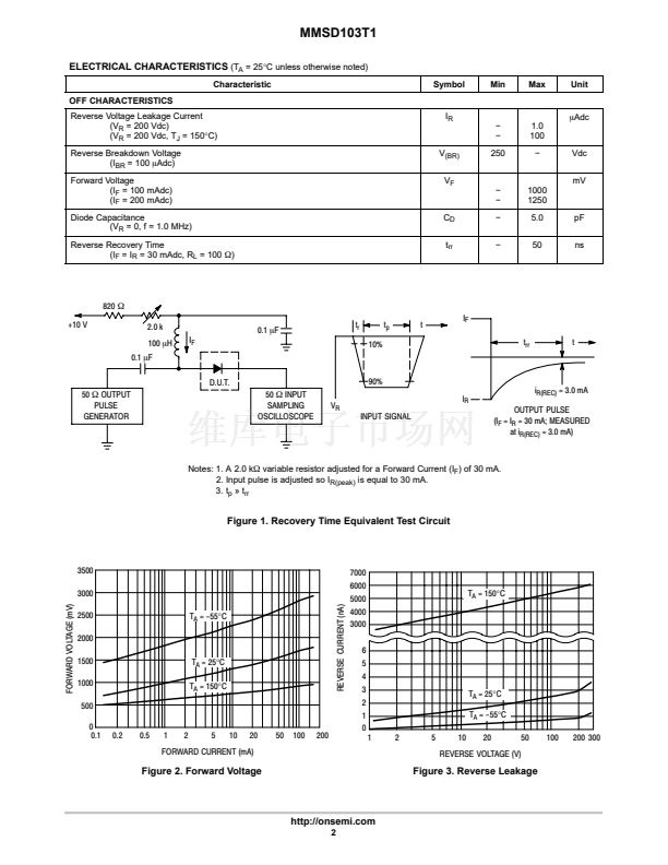
MAXIMUM RATINGS
Rating
Continuous Reverse Voltage
Peak Forward Current
Peak Forward Surge Current
Symbol
V
R
I
F
I
FM(surge)
Value
250
200
625
Unit
Vdc
mAdc
mAdc
http://onsemi.com
1
Cathode
2
Anode
2
1
THERMAL CHARACTERISTICS
Characteristic
Forward Power Dissipation, FR鈭? Board
(Note 1) @ T
A
= 25掳C
Derate above 25掳C
Thermal Resistance, Junction鈭抰o鈭扖ase
Thermal Resistance, Junction鈭抰o鈭扐mbient
Junction and Storage
Temperature Range
Symbol
P
F
400
3.2
R
qJL
R
qJA
T
J,
T
stg
174
492
鈭?5 to +150
mW
mW/掳C
掳C/W
掳C/W
掳C
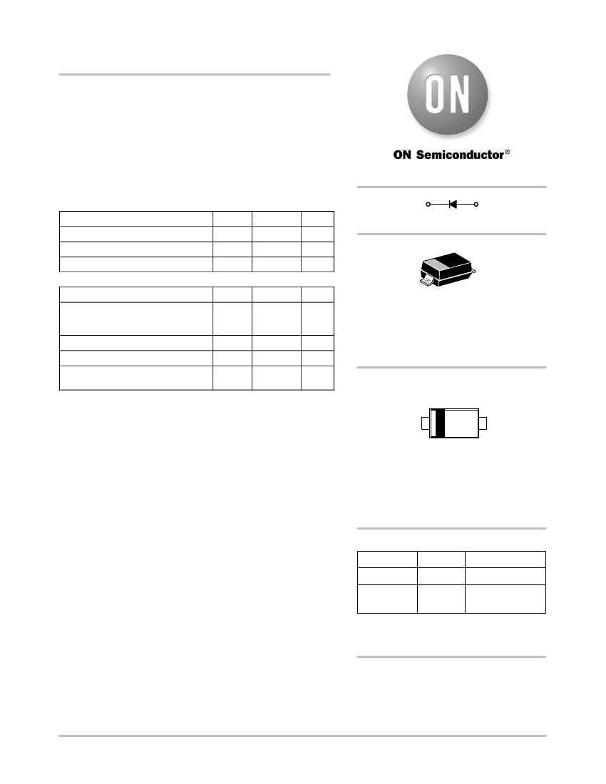
SOD鈭?23
CASE 425
STYLE 1
Value
Unit
MARKING DIAGRAM
Stresses exceeding Maximum Ratings may damage the device. Maximum
Ratings are stress ratings only. Functional operation above the Recommended
Operating Conditions is not implied. Extended exposure to stresses above the
Recommended Operating Conditions may affect device reliability.
1. FR鈭? = 1.0
�
0.75
�
0.062 in.
1
JS M
G
G
JS = Device Code
M = Date Code
G
= Pb鈭扚ree Package
(Note: Microdot may be in either location)
ORDERING INFORMATION
Device
MMSD103T1
MMSD103T1G
Package
SOD鈭?23
SOD鈭?23
(Pb鈭扚ree)
Shipping
鈥?/div>
3000 / Tape & Reel
3000 / Tape & Reel
鈥燜or information on tape and reel specifications,
including part orientation and tape sizes, please
refer to our Tape and Reel Packaging Specifications
Brochure, BRD8011/D.
Preferred
devices are recommended choices for future use
and best overall value.
漏
Semiconductor Components Industries, LLC, 2007
1
January, 2007 鈭?Rev. 3
Publication Order Number:
MMSD103T1/D


 1
1
 2
2
 3
3
