NE56610/11/12 Series
System Reset
Rev 0
February, 2001
Preliminary Product Specification
General Description
The NE56610/11/12 series is a family of devices designed to generate a reset signal for a
variety of microprocessor and logic systems. Accurate reset signals are generated during
momentary power interruptions or when ever power supply voltages sag to intolerable levels.
The NE56610/11/12 incorporates an internal timer to provide reset delay and ensure proper
operating voltage has been attained. In addition, a manual reset pin is available. An Open
Collector output topology is incorporated to provide adaptability for a wide variety of logic and
microprocessor systems.
NE56610/11/12 is available in the TSSOP5 surface mount package.
M/R
SUB
GND
1
2
3
4
5
V
CC
V
OUT
TSSOP5
Features
鈥?12V DC Maximum Operating Voltage
鈥?Low Operating Voltage (0.65 V)
鈥?Internal Reset Delay Timer
鈥?NE56610 (50 mS Typical)
鈥?NE56611 (100mS Typical)
鈥?NE56612 (200mS Typical)
鈥?Offered in Reset Thresholds of 2.0, 2.7, 2.8, 2.9, 3.0, 3.1, 4.2,
4.3, 4.4, 4.5, 4.7 V DC
鈥?Available in SSOP5 Surface Mount Package
鈥?Manual Reset Input
Applications
鈥?Micro-Computer Systems
鈥?Logic Systems
鈥?Battery Monitoring Systems
鈥?Back-Up Power Supply Circuits
鈥?Voltage Detection Circuits
鈥?Mechanical Reset Circuits
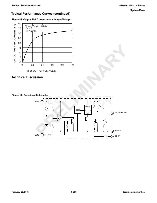
Simplified Device Diagram
V
CC
5
NE56610/11/12
4
V
OUT
Reset
Delay
+
GND
M/R
3
V
REF
1
2
SUB
Ordering Information
Description
5-pin SOT23 (TSSOP5) plastic surface mount
System Reset (100mS Typical Internal Reset Delay)
System Reset (200mS Typical Internal Reset Delay)
Temperature Range
-20 - +75
掳C
-20 - +75
掳C
-20 - +75
掳C
Order Code
NE56610-xxGW
NE56611-xxGW
NE56612-xxGW
DWG#
TSSOP5
TSSOP5
TSSOP5
Note: Each device has 6 (six) detection voltage options, indicated by the -xx on the order code:
XX
-25
-27
-29
Detect Voltage (Typ.)
2.5
2.7
2.9
XX
-39
-42
-45
Detect Voltage (Typ.)
3.9
4.2
4.5


 1
1
 2
2
 3
3
 4
4
 5
5
 6
6
 7
7
 8
8
 9
9
