鈮?/div>
10
ms)
Thermal Resistance 鈭?Junction鈭抰o鈭扐mbient
(Note 1)
Total Power Dissipation @ T
A
= 25掳C
Drain Current 鈭?Continuous @ T
A
= 25掳C
Thermal Resistance 鈭?Junction鈭抰o鈭扐mbient
(Note 2)
Total Power Dissipation @ T
A
= 25掳C
Drain Current 鈭?Continuous @ T
A
= 25掳C
Operating and Storage Temperature Range
Maximum Lead Temperature for Soldering
Purposes, 1/8鈥?from case for 10 seconds
Symbol
V
DSS
V
GS
R
qJC
P
D
I
D
I
D
I
D
R
qJA
P
D
I
D
R
qJA
P
D
I
D
T
J
, T
stg
T
L
Value
25
卤20
3.0
50
45
32
100
71.4
2.1
9.2
100
1.5
7.8
鈭?5 to
175
260
Unit
Vdc
Vdc
掳C/W
W
A
A
A
掳C/W
W
A
掳C/W
W
A
掳C
掳C
http://onsemi.com
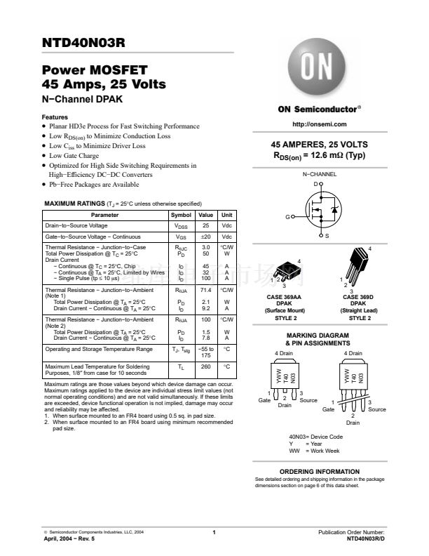
45 AMPERES, 25 VOLTS
R
DS(on)
= 12.6 mW (Typ)
N鈭扖HANNEL
D
G
S
4
4
1 2
3
CASE 369AA
DPAK
(Surface Mount)
STYLE 2
1
2
3
CASE 369D
DPAK
(Straight Lead)
STYLE 2
MARKING DIAGRAM
& PIN ASSIGNMENTS
4 Drain
YWW
T40
N03
4 Drain
YWW
T40
N03
3
Source
1
Gate
2
Drain
40N03= Device Code
Y
= Year
WW = Work Week
3
Source
Publication Order Number:
NTD40N03R/D
Maximum ratings are those values beyond which device damage can occur.
Maximum ratings applied to the device are individual stress limit values (not
normal operating conditions) and are not valid simultaneously. If these limits
are exceeded, device functional operation is not implied, damage may occur
and reliability may be affected.
1. When surface mounted to an FR4 board using 0.5 sq. in pad size.
2. When surface mounted to an FR4 board using minimum recommended
pad size.
1
Gate
2
Drain
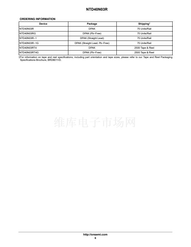
ORDERING INFORMATION
See detailed ordering and shipping information in the package
dimensions section on page 6 of this data sheet.
漏
Semiconductor Components Industries, LLC, 2004
1
April, 2004 鈭?Rev. 5


 1
1
 2
2
 3
3
 4
4
 5
5
 6
6
 7
7
 8
8
