鈥?/div>
Power Management in Portable and Battery鈥揚owered Products; i.e.,
Cellular and Cordless Telephones and PCMCIA Cards
4.9 AMPS
30 VOLTS
R
DS(on)
= 35 mW
D
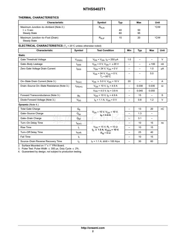
MAXIMUM RATINGS
(T
A
= 25掳C unless otherwise noted)
Rating
Drain鈥揝ource Voltage
Gate鈥揝ource Voltage
Continuous Drain Current
(T
J
= 150掳C) (Note 1.)
T
A
= 25掳C
T
A
= 85掳C
Pulsed Drain Current
Continuous Source Current
(Diode Conduction) (Note 1.)
Maximum Power Dissipation
(Note 1.)
T
A
= 25掳C
T
A
= 85掳C
Operating Junction and Storage
Temperature Range
Symbol
V
DS
V
GS
I
D
"6.7
"4.8
I
DM
I
S
P
D
2.5
1.3
T
J
, T
stg
1.3
0.7
掳C
2.1
"20
1.1
"4.9
"3.5
A
A
W
5 secs
30
"20
Steady
State
Unit
V
V
A
G
S
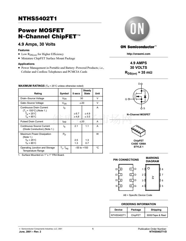
N鈥揅hannel MOSFET
鈥?5 to +150
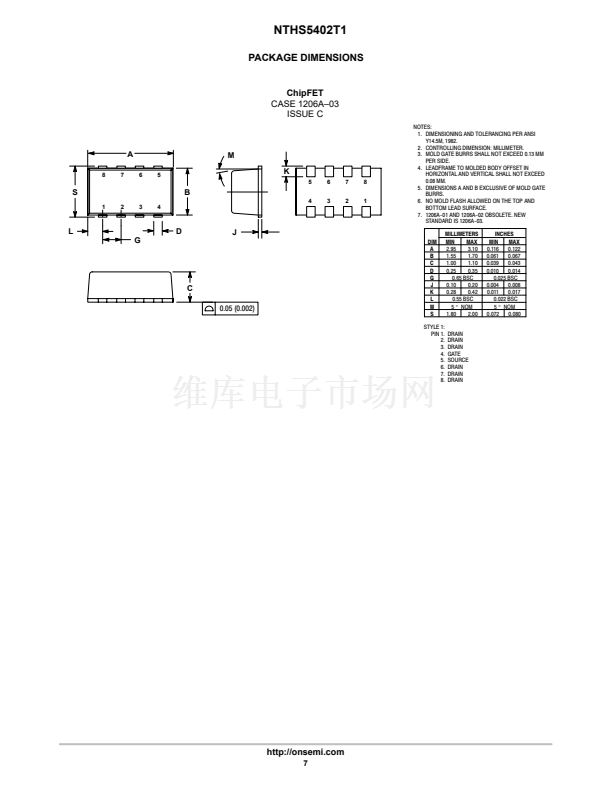
ChipFET
CASE 1206A
STYLE 1
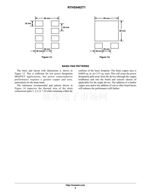
1. Surface Mounted on 1鈥?x 1鈥?FR4 Board.
PIN CONNECTIONS
MARKING
DIAGRAM
1
2
3
4
A8
8
7
6
5
D
D
D
S
8
7
6
5
1
2
3
4
D
D
D
G
A8 = Specific Device Code
ORDERING INFORMATION
Device
NTHS5402T1
Package
ChipFET
Shipping
3000/Tape & Reel
漏
Semiconductor Components Industries, LLC, 2001
1
June, 2001 鈥?Rev. 2
Publication Order Number:
NTHS5402T1/D


 1
1
 2
2
 3
3
 4
4
 5
5
 6
6
 7
7
 8
8
