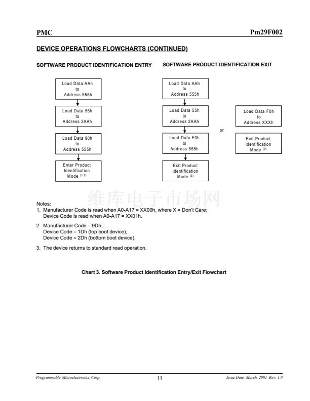
鈥?/div>
Single Power Supply Operation
- 5.0 V 卤 10% Read/Program/Erase
鈥?High Performance Read
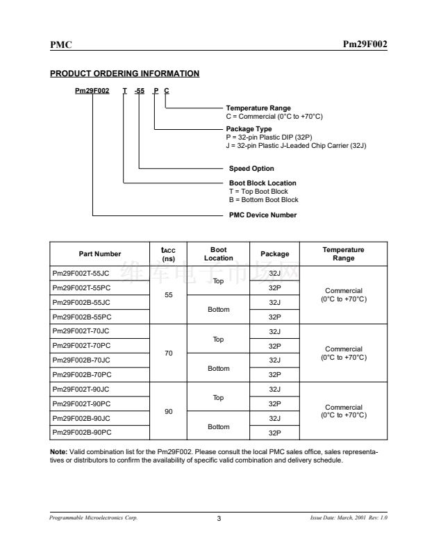
- 55/70/90 ns access time
鈥?Cost Effective Block Architecture
- One 16 Kbytes top or bottom Boot Block with
software lockout
- Two 8 Kbytes Parameter Blocks
- One 96 Kbytes Main Block
- One 128 Kbytes Main Block
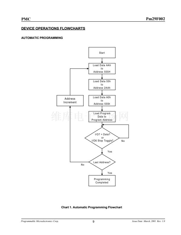
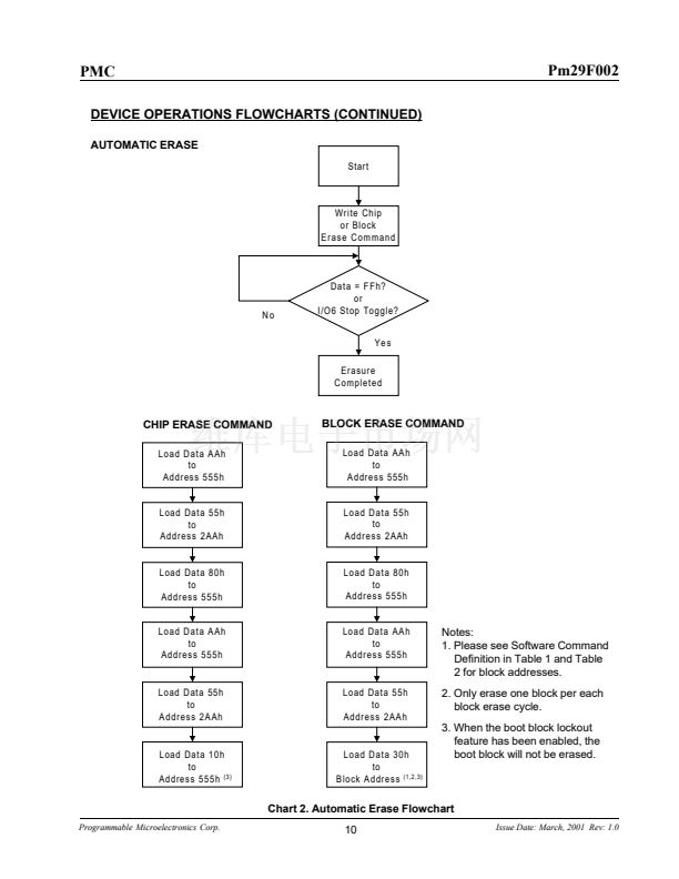
鈥?Automatic Erase and Program
-
Typical 15
碌s/byte
programming
- Typical 40 ms block or chip erase
鈥?Hardware Data Protection
ADVANCE INFORMATION
Pm29F002
2 Megabit (256K X 8) 5.0 Volt-only CMOS Flash Memory
鈥?Data# Polling and Toggle Bit Features
鈥?Low Power Consumption
- Typical 10 mA active read current
- Typical 40 mA program/erase current
- Typical <0.1
碌A
CMOS standby current
鈥?High Product Endurance
- Guarantee 10,000 program/erase cycles
- Typical 50,000 program/erase cycles
- Minimum 10 years data retention
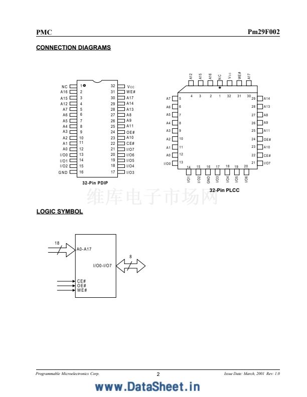
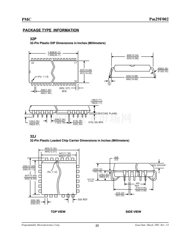
鈥?Industrial Standard Pin-out and Packaging
- 32-pin Plastic DIP
- 32-pin PLCC
鈥?Manufactured on 0.30 碌m process
- Fully compatible with previous 0.35 碌m version
GENERAL DESCRIPTION
The Pm29F002 is a 2 Megabit, 5.0 Volt-only Flash Memory organized as 262,144 bytes of 8 bits each.
This device is designed to use a 5.0 Volt power supply to perform in-system programming, 12.0 Volt V
PP
power
supply for program and erase operation is not required. The device can be programmed in standard EPROM
programmers as well.
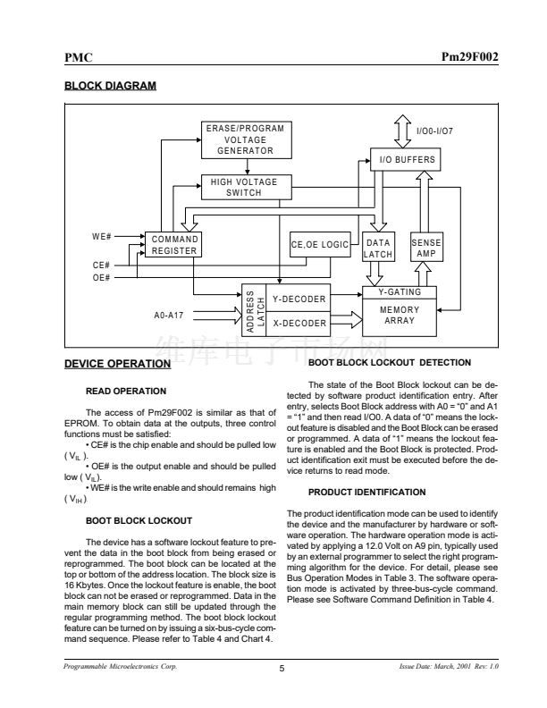
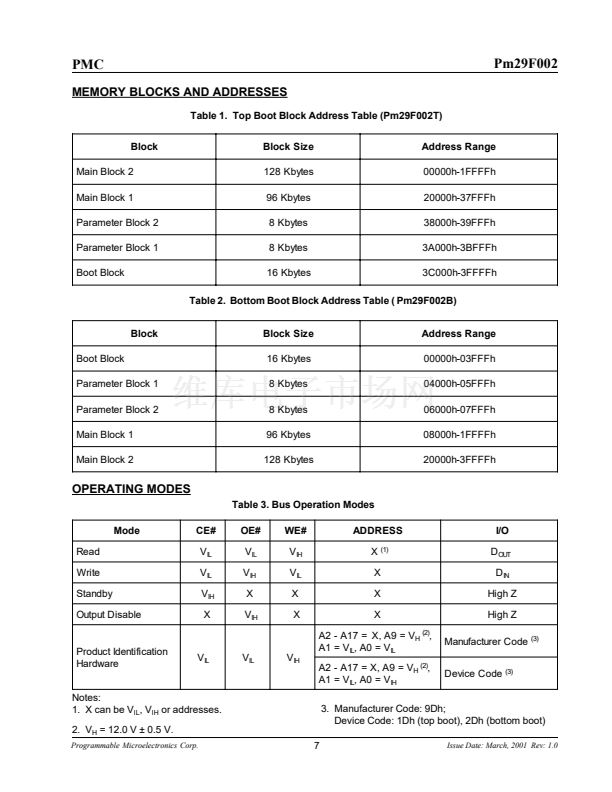
The 2 Megabit memory array is divided into five blocks of one 16 Kbytes, two 8 Kbytes, one 96 Kbytes, and
one 128 Kbytes for BIOS and parameters storage. The five blocks allow users to flexibly make chip erase or
block erase operation flexible. The block erase feature allows a particular block to be erased and reprogrammed
without affecting the data in other blocks. After the device performed chip erase or block erase operation, it can
be reprogrammed on a byte-by-byte basis.
The device has a standard microprocessor interface as well as JEDEC single-power-supply Flash compatible
pin-out and command set. The program operation of Pm29F002 is executed by issuing the program command
code into command register. The internal control logic automatically handles the programming voltage ramp-up
and timing. The erase operation of Pm29F002 is executed by issuing the chip erase or block erase command
code into command register. The internal control logic automatically handles the erase voltage ramp-up and
timing. The preprogramming on the array which has not been programmed is not required before the erase
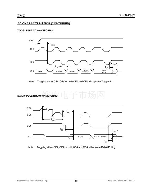
operation. The device also features Data# Polling and Toggle Bit function, the end of program or erase operation
can be detected by Data# Polling of I/O7 or Toggle Bit of I/O6.
The device has an optional 16 Kbytes top or bottom boot block with a software lockout feature for data
security. The boot block can be used to store user secure code. When the lockout feature is enabled, the boot
block is permanently protected from being reprogrammed.
The Pm29F002 is manufactured on PMC鈥檚 0.30 碌m advanced nonvolatile technology, P-FLASH鈩? The
device is packaged in a 32-pin DIP and PLCC with access time of 55, 70 and 90 ns.
Programmable Microelectronics Corp.
1
Issue Date: March, 2001 Rev:1.0


 1
1
 2
2
 3
3
 4
4
 5
5
 6
6
 7
7
 8
8
 9
9
 10
10
 11
11
 12
12
 13
13
 14
14
 15
15
 16
16
 17
17
 18
18
 19
19
 20
20
 21
21
