MITSUBISHI RF POWER MOS FET
ELECTROSTATIC SENSITIVE DEVICE
OBSERVE HANDLING PRECAUTIONS
RD20HMF1
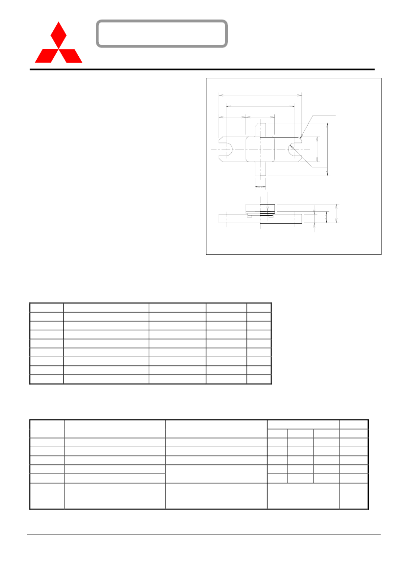
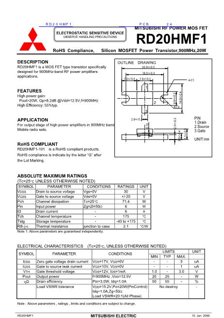
DRAWING
22.0+/-0.3
18.0+/-0.3
7.2+/-0.5
7.6+/-0.3
4-C1
RoHS Compliance,
DESCRIPTION
Silicon MOSFET Power Transistor,900MHz,20W
OUTLINE
RD20HMF1 is a MOS FET type transistor specifically
designed for 900MHz-band RF power amplifiers
applications.
High power gain:
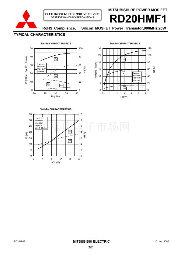
Pout>20W, Gp>8.2dB @Vdd=12.5V,f=900MHz
High Efficiency: 55%typ.
2
3
R1.6
14.0+/-0.4
6.6+/-0.3
FEATURES
1
APPLICATION
For output stage of high power amplifiers in 900MHz band
Mobile radio sets.
2.3+/-0.3
2.8+/-0.3
0.10
3.0+/-0.4
5.1+/-0.5
PIN
1.Drain
2.Source
3.Gate
UNIT:mm
RoHS COMPLIANT
RD20HMF1-101
is a RoHS compliant products.
RoHS compliance is indicate by the letter 鈥淕鈥?after
the Lot Marking.
ABSOLUTE MAXIMUM RATINGS
(Tc=25
掳C
UNLESS OTHERWISE NOTED)
SYMBOL
V
DSS
V
GSS
Pch
Pin
ID
Tch
Tstg
Rth j-c
PARAMETER
Drain to source voltage
Gate to source voltage
Channel dissipation
Input power
Drain current
Channel temperature
Storage temperature
Thermal resistance
CONDITIONS
Vgs=0V
Vds=0V
Tc=25
掳C
Zg=Zl=50
鈩?/div>
-
-
-
junction to case
RATINGS
30
+/-20
71.4
6
6
175
-40 to +175
2.1
UNIT
V
V
W
W
A
掳C
掳C
掳C/W
Note 1: Above parameters are guaranteed independently.
ELECTRICAL CHARACTERISTICS
SYMBOL
I
DSS
I
GSS
V
TH
Pout
畏D
PARAMETER
(Tc=25
掳C
, UNLESS OTHERWISE NOTED)
CONDITIONS
V
DS
=17V, V
GS
=0V
V
GS
=10V, V
DS
=0V
V
DS
=12V, I
DS
=1mA
f=900MHz ,V
DD
=12.5V
Pin=3.0W, Idq=1.0A
V
DD
=15.2V,Po=20W(PinControl)
Idq=1.0A,Zg=50
鈩?/div>
Load VSWR=20:1(All Phase)
MIN
-
-
1.0
20
50
LIMITS
TYP
MAX.
-
5
-
1
-
3.0
25
-
55
-
No destroy
UNIT
uA
uA
V
W
%
-
Zero gate voltage drain current
Gate to source leak current
Gate threshold voltage
Output power
Drain efficiency
Load VSWR tolerance
Note : Above parameters , ratings , limits and conditions are subject to change.
RD20HMF1
MITSUBISHI ELECTRIC
1/7
10 Jan 2006


 1
1
 2
2
 3
3
 4
4
 5
5
 6
6
 7
7
