鈩?/div>
Typical)
Low Input/Output Capacitance Minimizes
Loading and Signal Distortion
(C
io(OFF)
= 5 pF Typical)
Data and Control Inputs Provide
Undershoot Clamp Diodes
Low Power Consumption
(I
CC
= 3
碌A
Max)
V
CC
Operating Range From 4 V to 5.5 V
Data I/Os Support 0 to 5-V Signaling Levels
(0.8-V, 1.2-V, 1.5-V, 1.8-V, 2.5-V, 3.3-V, 5-V)
D
Control Inputs Can Be Driven by TTL or
D
D
D
5-V/3.3-V CMOS Outputs
I
off
Supports Partial-Power-Down Mode
Operation
Latch-Up Performance Exceeds 100 mA Per
JESD 78, Class II
ESD Performance Tested Per JESD 22
鈭?2000-V Human-Body Model
(A114-B, Class II)
鈭?1000-V Charged-Device Model (C101)
Supports Both Digital and Analog
Applications: USB Interface, Bus Isolation,
Low-Distortion Signal Gating
D
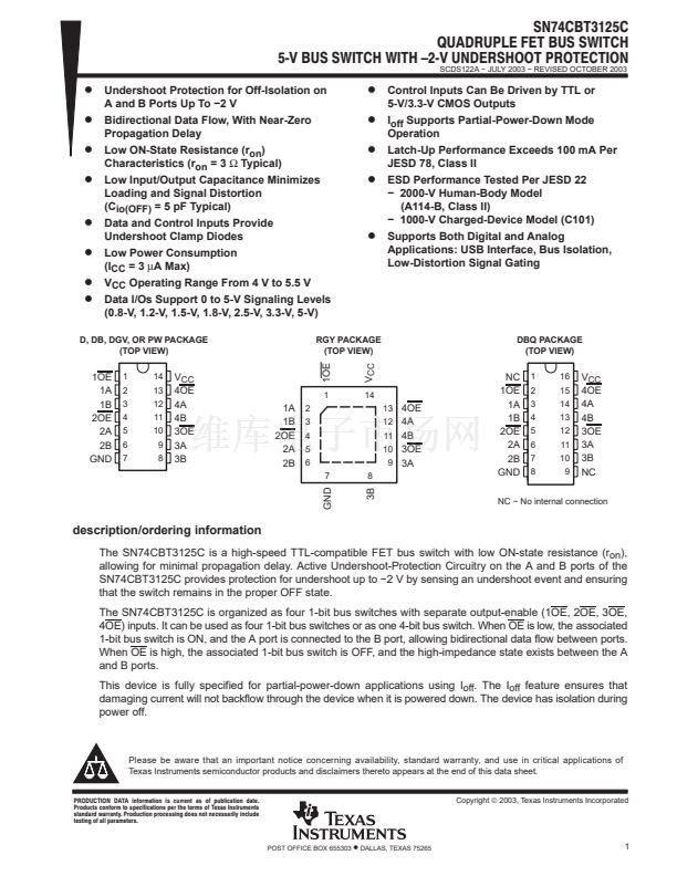
D, DB, DGV, OR PW PACKAGE
(TOP VIEW)
RGY PACKAGE
(TOP VIEW)
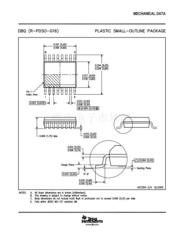
DBQ PACKAGE
(TOP VIEW)
1OE
V
CC
1OE
1A
1B
2OE
2A
2B
GND
1
2
3
4
5
6
7
14
13
12
11
10
9
8
V
CC
4OE
4A
4B
3OE
3A
3B
1
14
13
4OE
12
4A
11
4B
10
3OE
9
3A
1A
1B
2OE
2A
2B
2
3
4
5
6
7
8
NC
1OE
1A
1B
2OE
2A
2B
GND
1
2
3
4
5
6
7
8
16
15
14
13
12
11
10
9
V
CC
4OE
4A
4B
3OE
3A
3B
NC
GND
3B
NC 鈭?No internal connection
description/ordering information
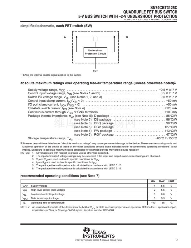
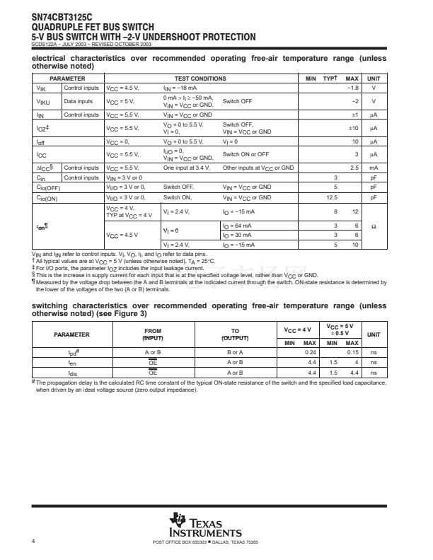
The SN74CBT3125C is a high-speed TTL-compatible FET bus switch with low ON-state resistance (r
on
),
allowing for minimal propagation delay. Active Undershoot-Protection Circuitry on the A and B ports of the
SN74CBT3125C provides protection for undershoot up to 鈭? V by sensing an undershoot event and ensuring
that the switch remains in the proper OFF state.
The SN74CBT3125C is organized as four 1-bit bus switches with separate output-enable (1OE, 2OE, 3OE,
4OE) inputs. It can be used as four 1-bit bus switches or as one 4-bit bus switch. When OE is low, the associated
1-bit bus switch is ON, and the A port is connected to the B port, allowing bidirectional data flow between ports.
When OE is high, the associated 1-bit bus switch is OFF, and the high-impedance state exists between the A
and B ports.
This device is fully specified for partial-power-down applications using I
off
. The I
off
feature ensures that
damaging current will not backflow through the device when it is powered down. The device has isolation during
power off.
Please be aware that an important notice concerning availability, standard warranty, and use in critical applications of
Texas Instruments semiconductor products and disclaimers thereto appears at the end of this data sheet.
PRODUCTION DATA information is current as of publication date.
Products conform to specifications per the terms of Texas Instruments
standard warranty. Production processing does not necessarily include
testing of all parameters.
Copyright
铮?/div>
2003, Texas Instruments Incorporated
POST OFFICE BOX 655303
鈥?/div>
DALLAS, TEXAS 75265
1


 1
1
 2
2
 3
3
 4
4
 5
5
 6
6
 7
7
 8
8
 9
9
 10
10
 11
11
 12
12
 13
13
 14
14
 15
15
