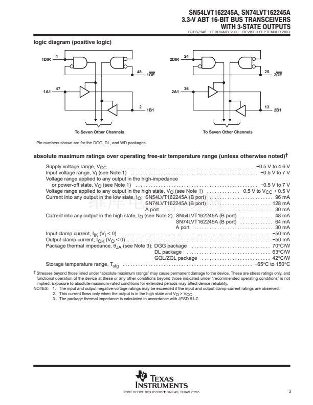
A-Port Outputs Have Equivalent 22-鈩?/div>
Series Resistors, So No External Resistors
Are Required
Support Mixed-Mode Signal Operation
(5-V Input and Output Voltages With
3.3-V V
CC
)
Support Unregulated Battery Operation
Down to 2.7 V
Typical V
OLP
(Output Ground Bounce)
<0.8 V at V
CC
= 3.3 V, T
A
= 25掳C
I
off
and Power-Up 3-State Support Hot
Insertion
Distributed V
CC
and GND Pins Minimize
High-Speed Switching Noise
Flow-Through Architecture Optimizes PCB
Layout
Latch-Up Performance Exceeds 100 mA Per
JESD 78, Class II
ESD Protection Exceeds JESD 22
鈭?2000-V Human-Body Model (A114-A)
鈭?200-V Machine Model (A115-A)
鈭?1000-V Charged-Device Model (C101)
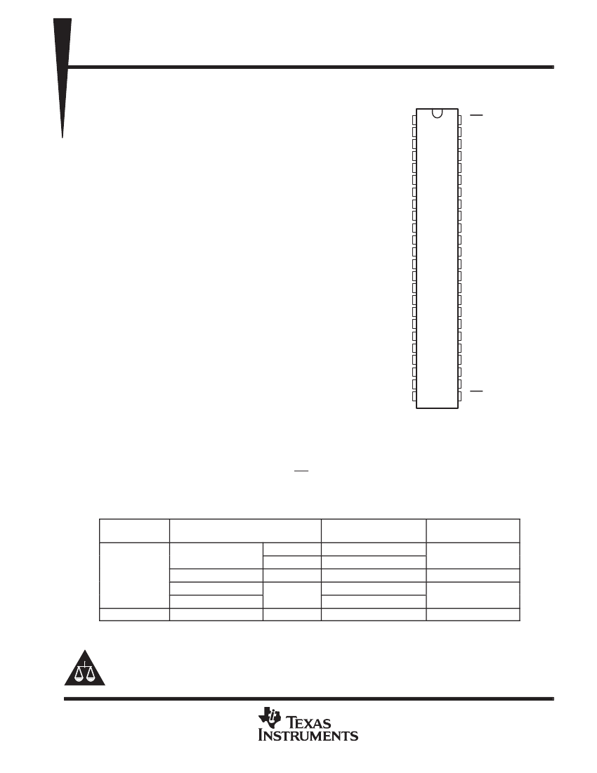
SN54LVT162245A . . . WD PACKAGE
SN74LVT162245A . . . DGG OR DL PACKAGE
(TOP VIEW)
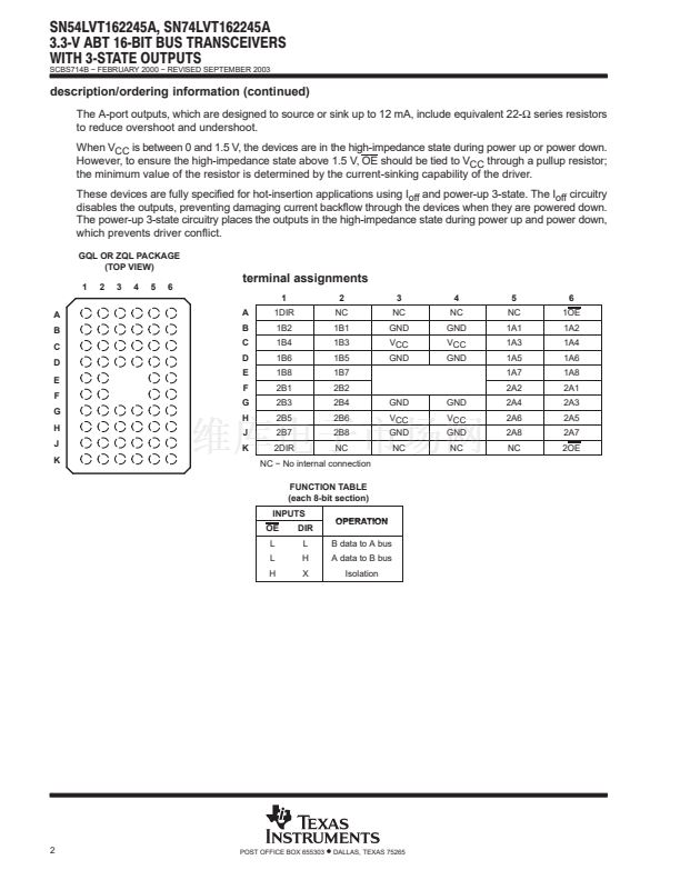
description/ordering information
1DIR
1B1
1B2
GND
1B3
1B4
V
CC
1B5
1B6
GND
1B7
1B8
2B1
2B2
GND
2B3
2B4
V
CC
2B5
2B6
GND
2B7
2B8
2DIR
1
2
3
4
5
6
7
8
9
10
11
12
13
14
15
16
17
18
19
20
21
22
23
24
48
47
46
45
44
43
42
41
40
39
38
37
36
35
34
33
32
31
30
29
28
27
26
25
1OE
1A1
1A2
GND
1A3
1A4
V
CC
1A5
1A6
GND
1A7
1A8
2A1
2A2
GND
2A3
2A4
V
CC
2A5
2A6
GND
2A7
2A8
2OE
The 鈥橪VT162245A devices are 16-bit (dual-octal) noninverting 3-state transceivers designed for low-voltage
(3.3-V) V
CC
operation, but with the capability to provide a TTL interface to a 5-V system environment.
These devices can be used as two 8-bit transceivers or one 16-bit transceiver. The devices allow data
transmission from the A bus to the B bus or from the B bus to the A bus, depending on the logic level at the
direction-control (DIR) input. The output-enable (OE) input can be used to disable the device so that the buses
are effectively isolated.
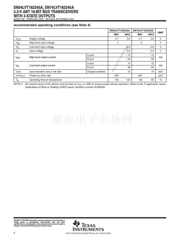
ORDERING INFORMATION
TA
SSOP 鈭?DL
鈭?0掳C to 85掳C
鈭?0 C 85 C
TSSOP 鈭?DGG
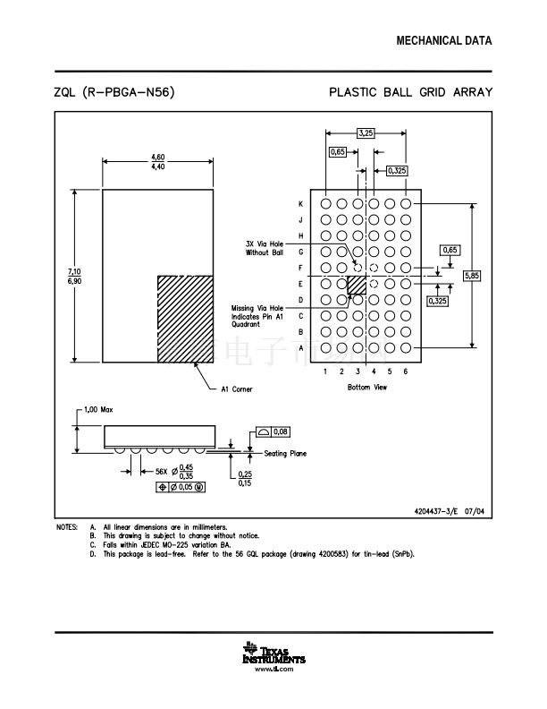
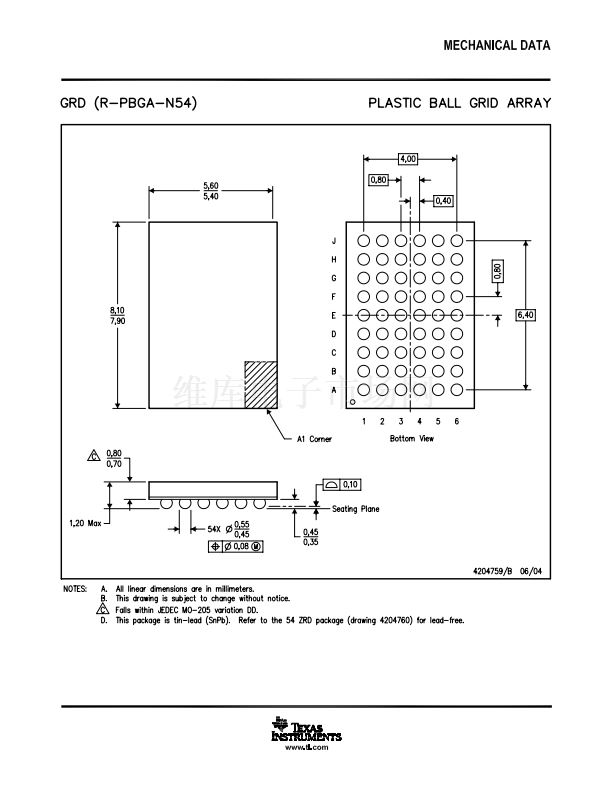
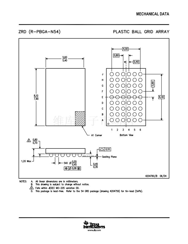
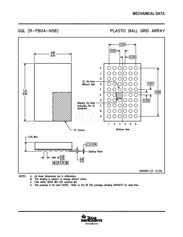
VFBGA 鈭?GQL
VFBGA 鈭?ZQL (Pb-free)
鈭?5掳C to 125掳C
CFP 鈭?WD
Tape and reel
Tube
PACKAGE鈥?/div>
Tube
Tape and reel
Tape and reel
ORDERABLE
PART NUMBER
SN74LVT162245ADL
SN74LVT162245ADLR
SN74LVT162245ADGGR
SN74LVT162245AGQLR
SN74LVT162245AZQLR
SNJ54LVT162245AWD
LZ245A
SNJ54LVT162245AWD
LVT162245A
LVT162245A
TOP-SIDE MARKING
鈥?Package drawings, standard packing quantities, thermal data, symbolization, and PCB design guidelines are available at
www.ti.com/sc/package.
Please be aware that an important notice concerning availability, standard warranty, and use in critical applications of
Texas Instruments semiconductor products and disclaimers thereto appears at the end of this data sheet.
Widebus is a trademark of Texas Instruments.
UNLESS OTHERWISE NOTED this document contains PRODUCTION
DATA information current as of publication date. Products conform to
specifications per the terms of Texas Instruments standard warranty.
Production processing does not necessarily include testing of all
parameters.
POST OFFICE BOX 655303
Copyright
铮?/div>
2003, Texas Instruments Incorporated
鈥?/div>
DALLAS, TEXAS 75265
1


 1
1
 2
2
 3
3
 4
4
 5
5
 6
6
 7
7
 8
8
 9
9
 10
10
 11
11
 12
12
 13
13
 14
14
 15
15
