(on) = 0.07鈩?/div>
EXCEPTIONAL dv/dt CAPABILITY
LOW GATE CHARGE AT 100
o
C
LOW THRESHOLD DRIVE
1
2
3
1
2
3
DESCRIPTION
This Power MOSFET is the latest development of
STMicroelectronis unique "Single Feature Size鈩?quot; strip-
based process. The resulting transistor shows extremely
high packing density for low on-resistance, rugged
avalanche characteristics and less critical alignment
steps
therefore
a
remarkable
manufacturing
reproducibility.
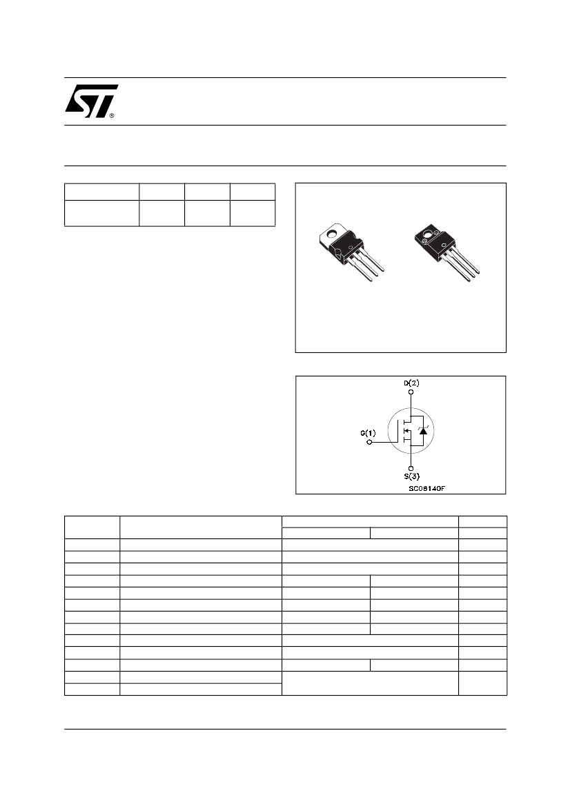
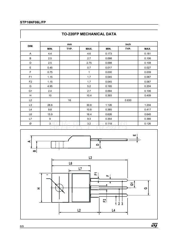
TO-220
TO-220FP
INTERNAL SCHEMATIC DIAGRAM
APPLICATIONS
s
MOTOR CONTROL, AUDIO AMPLIFIERS
s
HIGH CURRENT, HIGH SPEED SWITCHING
s
SOLENOID AND RELAY DRIVERS
s
DC-DC & DC-AC CONVERTERS
s
AUTOMOTIVE ENVIRONMENT
ABSOLUTE MAXIMUM RATINGS
Symbol
V
DS
V
DGR
V
GS
I
D
I
D
I
DM
(鈥?
P
tot
dv/dt
(1)
E
AS (2)
V
ISO
T
stg
T
j
Parameter
STP16NF06L
Drain-source Voltage (V
GS
= 0)
Drain-gate Voltage (R
GS
= 20 k鈩?
Gate- source Voltage
Drain Current (continuous) at T
C
= 25掳C
Drain Current (continuous) at T
C
= 100掳C
Drain Current (pulsed)
Total Dissipation at T
C
= 25掳C
Derating Factor
Peak Diode Recovery voltage slope
Single Pulse Avalanche Energy
Insulation Withstand Voltage (DC)
Storage Temperature
Operating Junction Temperature
16
11
64
45
0.3
23
127
--------
-55 to 175
2500
60
60
卤 16
11(*)
7.5(*)
44(*)
25
0.17
Value
STP16NF06LFP
V
V
V
A
A
A
W
W/掳C
V/ns
mJ
V
掳C
Unit
(鈥? Pulse width limited by safe operating area.
(*) Current Limited by package鈥檚 thermal resistance
(1) I
SD
鈮?/div>
16A, di/dt
鈮?/div>
210A/碌s, V
DD
鈮?/div>
V
(BR)DSS
, T
j
鈮?/div>
T
JMAX.
(2) Starting T
j
= 25
o
C, I
D
= 8A, V
DD
= 30V
August 2002
.
1/9


 1
1
 2
2
 3
3
 4
4
 5
5
 6
6
 7
7
 8
8
 9
9
