600ps max. propagation delay
鈩?/div>
input pulldown resistors
s
Fully compatible with Motorola MC10E/100E104
s
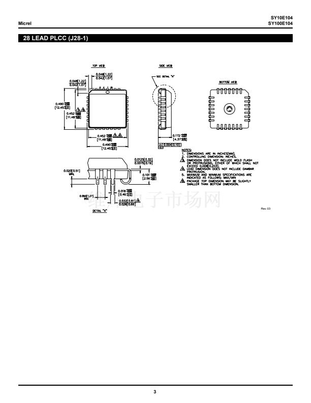
Available in 28-pin PLCC package
SY10E104
SY100E104
DESCRIPTION
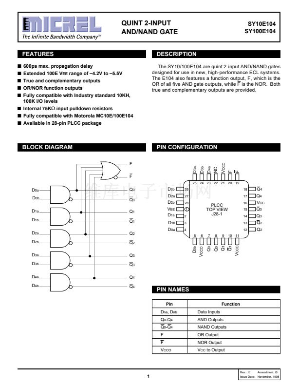
The SY10/100E104 are quint 2-input AND/NAND gates
designed for use in new, high-performance ECL systems.
The E104 also features a function output, F, which is the
OR of all five AND gate outputs, while F is the NOR. Both
true and complementary outputs are provided.
BLOCK DIAGRAM
F
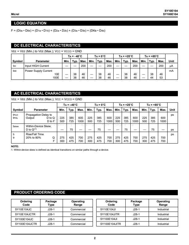
PIN CONFIGURATION
V
CCO
D
3a
D
3b
D
4a
NC
F
25 24 23 22 21 20
19
18
17
D
0a
D
0b
D
1a
D
1b
D
2a
D
2b
D
3a
D
3b
D
4a
D
4b
Q
0
Q
0
Q
1
Q
1
Q
2
Q
2
Q
3
Q
3
Q
4
Q
4
D
3b
D
2a
D
2b
V
EE
D
1a
D
1b
D
0a
F
F
26
27
28
1
2
3
4
5
6
7
8
9
10
11
Q
4
Q
4
V
CC
Q
3
Q
3
Q
2
Q
2
PLCC
TOP VIEW
J28-1
16
15
14
13
12
PIN NAMES
Pin
D
na
, D
nb
Q
0
-Q
4
Q
0
-Q
4
F
F
V
CCO
Data Inputs
AND Outputs
NAND Outputs
OR Output
NOR Output
V
CC
to Output
Function
V
CCO
V
CCO
Rev.: E
D
0b
Q
0
Q
0
Q
1
Q
1
Amendment: /0
1
Issue Date: November, 1998


 1
1
 2
2
 3
3
 4
4
