鈥?/div>
Pb鈭扚ree Package is Available*
MAXIMUM RATINGS
(T
J
= 25掳C unless otherwise noted)
Rating
Peak Repetitive Off鈭扴tate Voltage (Note 1)
(T
J
= 鈭?0 to +125掳C, Gate Open)
On鈭扴tate RMS Current
(All Conduction Angles, T
C
= +80掳C)
Peak Non鈭扲epetitive Surge Current (One
Full Cycle Sine Wave, 60 Hz, T
J
= +80掳C)
Circuit Fusing Consideration (t = 8.3 ms)
Peak Gate Power
(Pulse Width = 10
ms,
T
C
= +80掳C)
Average Gate Power
(t = 8.3 ms, T
C
= +80掳C)
Peak Gate Current
(Pulse Width = 10
ms,
T
C
= +80掳C)
Operating Junction Temperature Range
Storage Temperature Range
Symbol
V
DRM,
V
RRM
I
T(RMS)
I
TSM
I
2
t
P
GM
P
G(AV)
I
GM
T
J
T
stg
Value
400
8.0
100
40
16
0.35
4.0
鈭?0 to +125
鈭?0 to +150
Unit
V
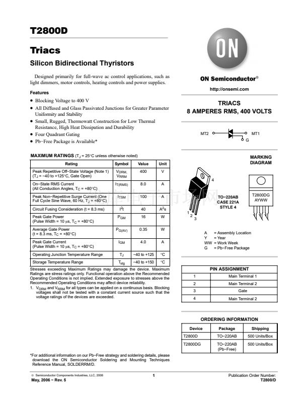
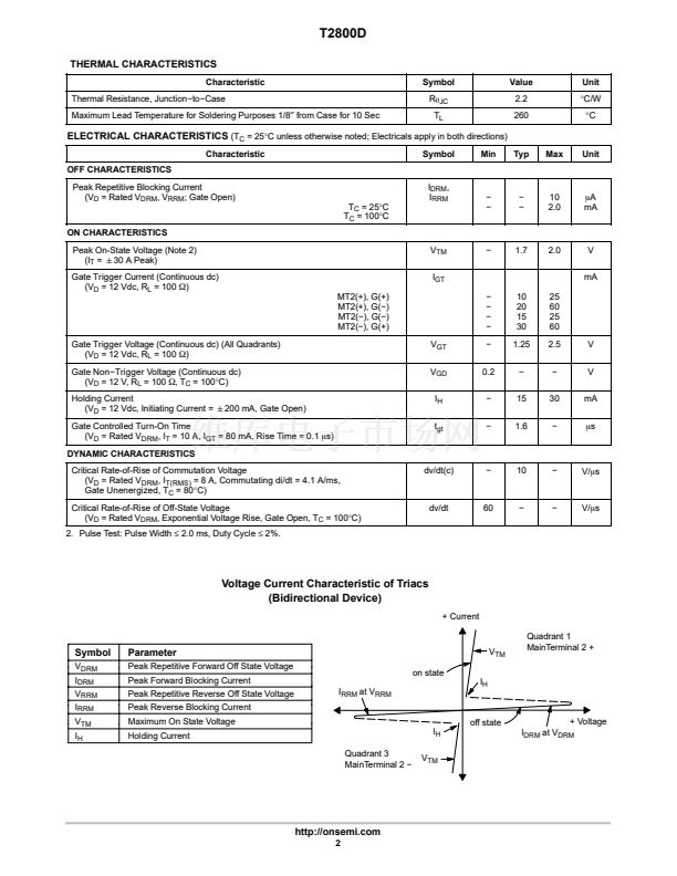
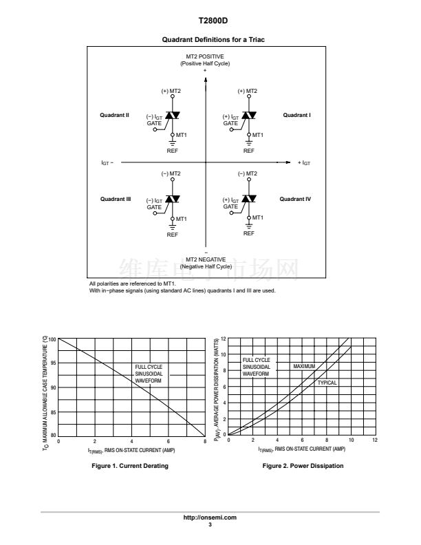
TRIACS
8 AMPERES RMS, 400 VOLTS
MT2
G
MT1
MARKING
DIAGRAM
4
A
A
A
2
s
W
W
A
掳C
掳C
A
Y
WW
G
= Assembly Location
= Year
= Work Week
= Pb鈭扚ree Package
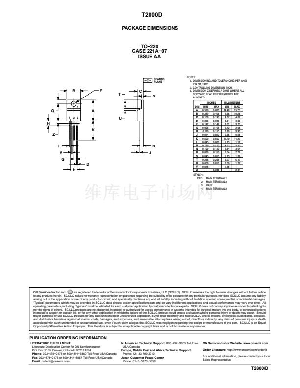
TO鈭?20AB
CASE 221A
STYLE 4
1
2
3
T2800DG
AYWW
Stresses exceeding Maximum Ratings may damage the device. Maximum
Ratings are stress ratings only. Functional operation above the Recommended
Operating Conditions is not implied. Extended exposure to stresses above the
Recommended Operating Conditions may affect device reliability.
1. V
DRM
and V
RRM
for all types can be applied on a continuous basis. Blocking
voltages shall not be tested with a constant current source such that the
voltage ratings of the devices are exceeded.
PIN ASSIGNMENT
1
2
3
4
Main Terminal 1
Main Terminal 2
Gate
Main Terminal 2
ORDERING INFORMATION
Device
T2800D
T2800DG
*For additional information on our Pb鈭扚ree strategy and soldering details, please
download the ON Semiconductor Soldering and Mounting Techniques
Reference Manual, SOLDERRM/D.
漏
Semiconductor Components Industries, LLC, 2006
Package
TO鈭?20AB
TO鈭?20AB
(Pb鈭扚ree)
Shipping
500 Units/Box
500 Units/Box
1
May, 2006 鈭?Rev. 5
Publication Order Number:
T2800/D


 1
1
 2
2
 3
3
 4
4
