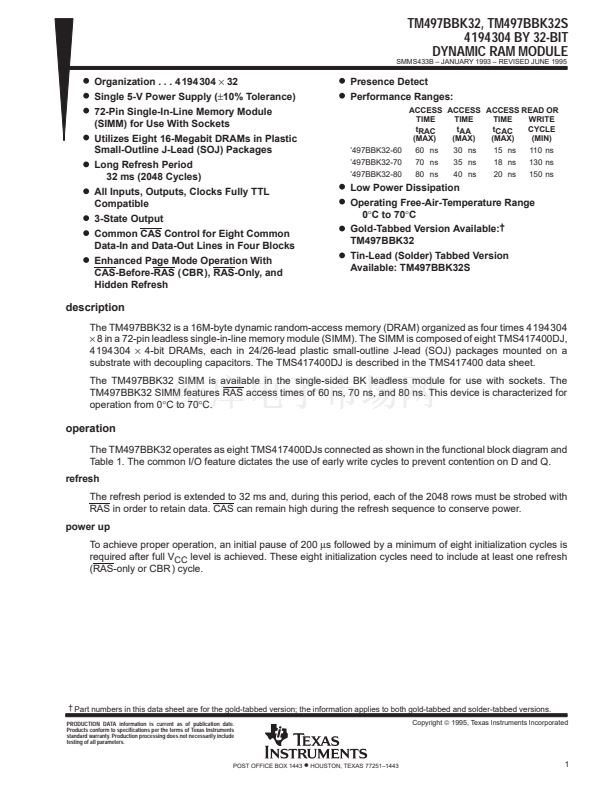
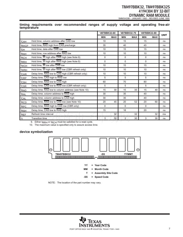
TM497BBK32, TM497BBK32S
4194304 BY 32-BIT
DYNAMIC RAM MODULE
SMMS433B 鈥?JANUARY 1993 鈥?REVISED JUNE 1995
D
D
D
D
D
D
D
D
D
Organization . . . 4 194 304
脳
32
Single 5-V Power Supply (卤10% Tolerance)
72-Pin Single-In-Line Memory Module
(SIMM) for Use With Sockets
Utilizes Eight 16-Megabit DRAMs in Plastic
Small-Outline J-Lead (SOJ) Packages
Long Refresh Period
32 ms (2048 Cycles)
All Inputs, Outputs, Clocks Fully TTL
Compatible
3-State Output
Common CAS Control for Eight Common
Data-In and Data-Out Lines in Four Blocks
Enhanced Page Mode Operation With
CAS-Before-RAS ( CBR), RAS-Only, and
Hidden Refresh
D
D
Presence Detect
Performance Ranges:
ACCESS ACCESS ACCESS READ OR
TIME
TIME
TIME
WRITE
tRAC
tAA
tCAC
CYCLE
(MAX)
(MAX)
(MAX)
(MIN)
鈥?97BBK32-60
60 ns
30 ns
15 ns
110 ns
鈥?97BBK32-70
70 ns
35 ns
18 ns
130 ns
鈥?97BBK32-80
80 ns
40 ns
20 ns
150 ns
D
D
D
D
Low Power Dissipation
Operating Free-Air-Temperature Range
0掳C to 70掳C
Gold-Tabbed Version Available:
鈥?/div>
TM497BBK32
Tin-Lead (Solder) Tabbed Version
Available: TM497BBK32S
description
The TM497BBK32 is a 16M-byte dynamic random-access memory (DRAM) organized as four times 4 194 304
脳
8 in a 72-pin leadless single-in-line memory module (SIMM). The SIMM is composed of eight TMS417400DJ,
4 194 304
脳
4-bit DRAMs, each in 24/26-lead plastic small-outline J-lead (SOJ) packages mounted on a
substrate with decoupling capacitors. The TMS417400DJ is described in the TMS417400 data sheet.
The TM497BBK32 SIMM is available in the single-sided BK leadless module for use with sockets. The
TM497BBK32 SIMM features RAS access times of 60 ns, 70 ns, and 80 ns. This device is characterized for
operation from 0掳C to 70掳C.
operation
The TM497BBK32 operates as eight TMS417400DJs connected as shown in the functional block diagram and
Table 1. The common I/O feature dictates the use of early write cycles to prevent contention on D and Q.
refresh
The refresh period is extended to 32 ms and, during this period, each of the 2048 rows must be strobed with
RAS in order to retain data. CAS can remain high during the refresh sequence to conserve power.
power up
To achieve proper operation, an initial pause of 200
碌s
followed by a minimum of eight initialization cycles is
required after full V
CC
level is achieved. These eight initialization cycles need to include at least one refresh
(RAS-only or CBR ) cycle.
鈥?Part numbers in this data sheet are for the gold-tabbed version; the information applies to both gold-tabbed and solder-tabbed versions.
PRODUCTION DATA information is current as of publication date.
Products conform to specifications per the terms of Texas Instruments
standard warranty. Production processing does not necessarily include
testing of all parameters.
Copyright
漏
1995, Texas Instruments Incorporated
POST OFFICE BOX 1443
鈥?/div>
HOUSTON, TEXAS 77251鈥?443
1


 1
1
 2
2
 3
3
 4
4
 5
5
 6
6
 7
7
 8
8
 9
9
