鈥?/div>
Interchangeable with SG1524,
SG2524 and SG3524, Respectively
DESCRIPTION
The UC1524, UC2524 and UC3524 incorporate on a single monolithic chip
all the functions required for the construction of regulating power supplies, in-
verters or switching regulators. They can also be used as the control element
for high-power-output applications. The UC1524 family was designed for
switching regulators of either polarity, transformer-coupled dc-to-dc convert-
ers, transformerless voltage doublers and polarity converter applications em-
ploying fixed-frequency, pulse-width modulation techniques. The dual
alternating outputs allow either single-ended or push-pull applications. Each
device includes an on-chip reference, error amplifier, programmable oscilla-
tor, pulse-steering flip-flop, two uncommitted output transistors, a high-gain
comparator, and current-limiting and shut-down circuitry. The UC1524 is
characterized for operation over the full military temperature range of -55掳C
to +125掳C. The UC2524 and UC3524 are designed for operation from -25掳C
to +85掳C and 0掳 to +70掳C, respectively.
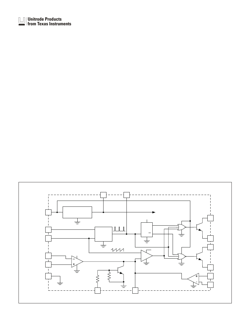
BLOCK DIAGRAM
V
REF
16
OSC OUT
3
V
IN
15
REFERENCE
REGULATOR
+5V
Q
+5V TO ALL
INTERNAL
CIRCUITRY
12
C
A
R
T
C
T
(RAMP)
6
OSC
7
R
Q
11
13
E
A
C
B
INV INPUT
NI INPUT
GROUND
(SUBSTRATE)
1
2
+5V
EA
+5V
COMPARATOR
14
10k
5
4
10
SHUTDOWN
9
COMPENSATION
E
B
鈥揝ENSE
+SENSE
8
1k
CL
SLUS180D - NOVEMBER 1999 - REVISED AUGUST 2002


 1
1
 2
2
 3
3
 4
4
 5
5
 6
6
 7
7
 8
8
