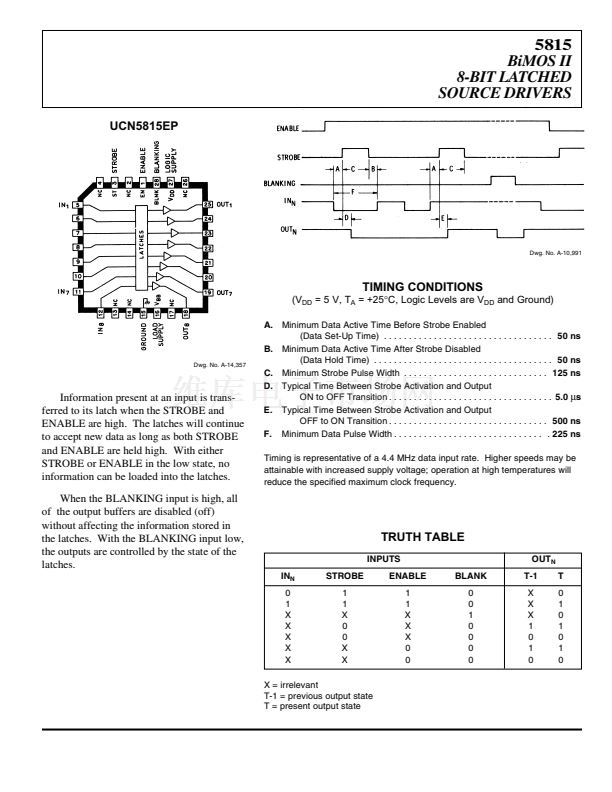
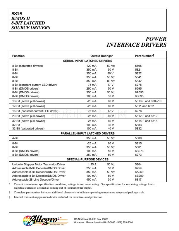
5815
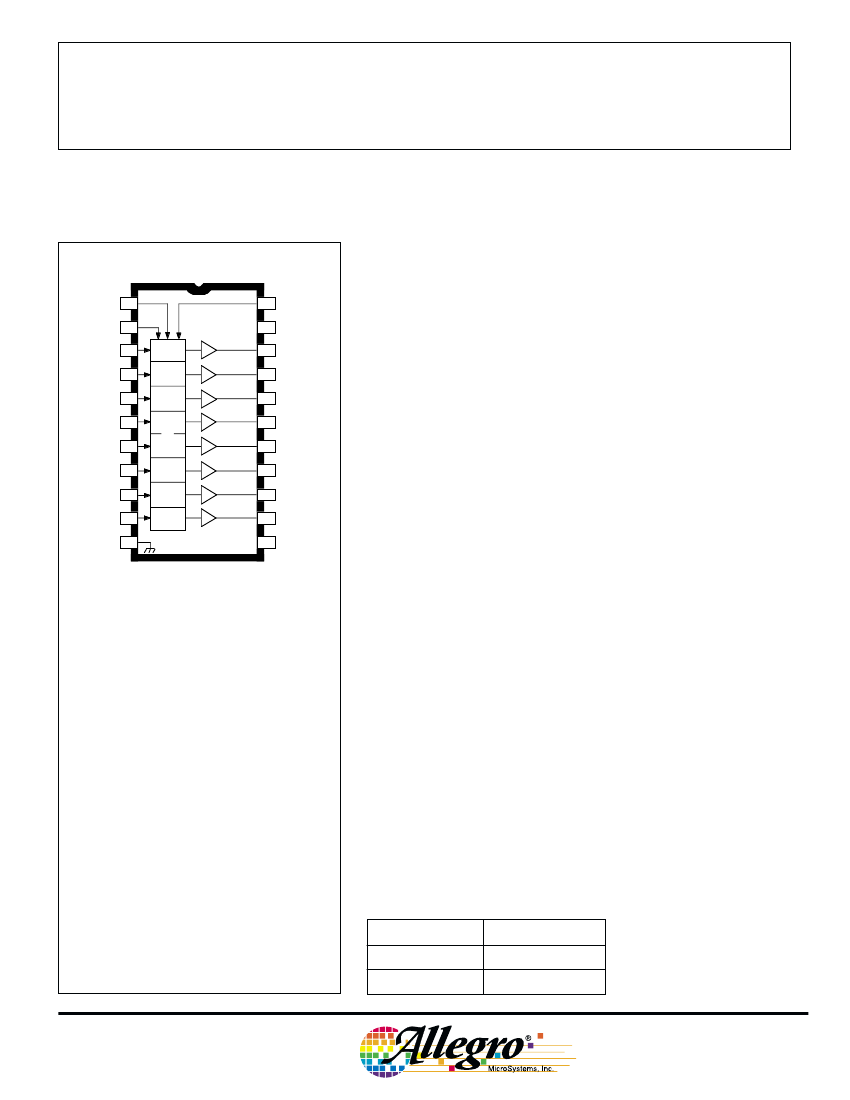
UCN5815A
ENABLE
STROBE
IN
1
IN
2
IN
3
IN
4
IN
5
IN
6
IN
7
IN
8
GROUND
1
2
3
4
5
6
7
8
9
10
11
LATCHES
BiMOS II 8-BIT
LATCHED SOURCE DRIVERS
Designed primarily for use with high-voltage vacuum-fluorescent
displays, the UCN5815A and UCN5815EP BiMOS II integrated
circuits consist of eight npn Darlington source drivers with output pull-
down resistors, a CMOS latch for each driver, and common STROBE,
BLANKING, and ENABLE functions.
BiMOS II devices have considerably better data-input rates than
the original BiMOS circuits. With a 5 V logic supply, they will operate
to at least 4.4 MHz. With a 12 V supply, significantly higher speeds
are obtained. The CMOS inputs cause minimum loading and are
compatible with standard CMOS and NMOS logic commonly found in
microprocessor designs. TTL circuits may require the use of appropri-
ate pull-up resistors.
The bipolar outputs may be used as segment, dot (matrix), bar, or
digit drivers in vacuum-fluorescent displays. All eight outputs can be
activated simultaneously at ambient temperatures in excess of 75掳C.
To simplify printed wiring board layout, output connections are
opposite the inputs. A minimum component display subsystem,
requiring few or no discrete components, can be assembled using the
UCN5815A/EP with the UCN5810AF/EPF/LWF, UCN5812AF/EPF,
or UCN5818AF/EPF serial-to-parallel latched drivers.
Suffix 鈥楢鈥?devices are furnished in a standard 22-pin plastic DIP;
suffix 鈥楨P鈥?indicates a 28-lead PLCC.
Data Sheet
26183.10A*
22
V
DD
21
20
19
18
17
16
15
14
13
V
BB
12
BLANKING
LOGIC
SUPPLY
OUT
1
OUT
2
OUT
3
OUT
4
OUT
5
OUT
6
OUT
7
OUT
8
LOAD
SUPPLY
Dwg. PP-015-3
ABSOLUTE MAXIMUM RATINGS
at +25掳C Free-Air Temperature
Output Voltage, V
OUT
. . . . . . . . . . . . . .
60 V
Logic Supply Voltage Range,
V
DD
. . . . . . . . . . . . . . . . . .
4.5 V to 15 V
Load Supply Voltage Range,
V
BB
. . . . . . . . . . . . . . . . . .
5.0 V to 60 V
Input Voltage Range,
V
IN
. . . . . . . . . . .
-0.3 V to V
DD
+ 0.3 V
Continuous Output Current,
I
OUT
. . . . . . . . . . . . . . . . . . . . . .
-40 mA
Package Power Dissipation, P
D
(UCN5815A) . . . . . . . . . . . . . . .
2.5 W*
(UCN5815EP) . . . . . . . . . . . . .
2.27 W*
Operating Temperature Range,
T
A
. . . . . . . . . . . . . . . . .
-20
掳
C to +85
掳
C
Storage Temperature Range,
T
S
. . . . . . . . . . . . . . . .
-55
掳
C to +150
掳
C
* Derate linearly to 0 W at +150掳C.
Caution: CMOS devices have input static
protection but are susceptible to damage
when exposed to extremely high static
electrical charges.
FEATURES
I
I
I
I
I
I
To 4.4 MHz Date-lnput Rate
High-Voltage Source Outputs
CMOS, NMOS, TTL Compatible Inputs
Low-Power CMOS Latches
Internal Pull-Down Resistors
Wide Supply-Voltage Range
Always order by complete part number:
Part Number
UCN5815A
UCN5815EP
Package
22-Pin DIP
28-Lead PLCC


 1
1
 2
2
 3
3
 4
4
 5
5
 6
6
