Maintenance only
Features
Description
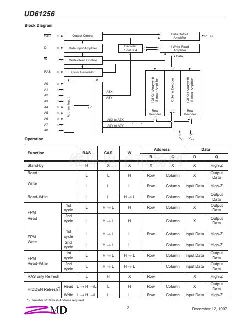
Addressing
The UD61256 is a dynamic Write-
Read-memory with random access.
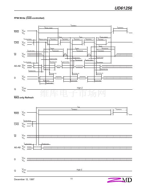
FPM facilitates faster data operation
with predefined row address. Via 9
address inputs the 18 address bits
are transmitted into the internal
address memories in a time-multi-
plex operation. The falling RAS-
edge takes over the row address.
During RAS Low, the column
address together with the CAS
signal are taken over. The selection
of one or more memory circuits can
be made by activation of the RAS
input.
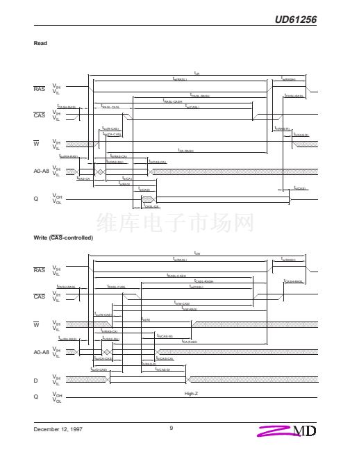
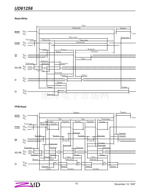
Read-Write-Control
The choice between Read or Write
cycle is made at the W input. HIGH
at the W input causes a Read cycle,
meanwhile LOW leads to a Write
cycle.
Both CAS-controlled and W-control-
led Write cycles are possible with
activated RAS signal.
UD61256
256K x 1 DRAM
Data Output Control
The usual state of the data output is
the High-Z state. Whenever CAS is
inactive (HIGH), Q will float (High-Z).
Thus, CAS functions as data output
control.
After access time, in case of a Read
cycle, the output is activated, and it
contains the logic 鈥?鈥?or 鈥?鈥?
Q is then valid until CAS returns into
to inactive state (HIGH).
The memory cycle being a Read,
Read-Write or a Write cycle (W-con-
trolled), Q changes from High-Z
state to the active state (鈥?鈥?or 鈥?鈥?.
After the access time the contents of
the selected cell is available, except
for the Write cycle.
The output remains active until CAS
becomes inactive, irrespective of
RAS becoming inactive or not. The
memory cycle being a Write cycle
(CAS-controlled), the data output
keeps its High-Z state throughout
the whole cycle. This configuration
makes Q fully controllable by the
user merely through the timing of W.
The output storaging the data, they
remain valid from the end of access
time until the start of another cycle.
F
Dynamic random access memory
F
F
F
F
F
F
F
F
F
F
262144 x 1 bit manufactured
using a CMOS technology
RAS access times 70 ns, 80 ns
TTL-compatible
Three-state output
256 refresh cycles
4 ms refresh cycle time
FAST PAGE MODE
Operating modes: Read, Write,
Read - Write,
RAS only Refresh,
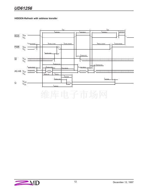
Hidden Refresh with address
transfer
Power Supply Voltage 5 V
Packages PDIP16 (300 mil)
SOJ20/26 (300 mil)
Operating temperature range
0 to 70 掳C
Quality assessment according to
CECC 90000, CECC 90100 and
CECC 90112
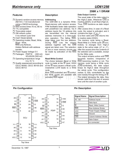
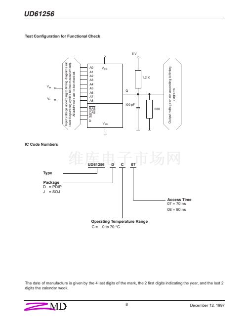
Pin Configuration
Pin Description
A8
D
W
RAS
n.c.
1
2
3
4
5
26
25
24
23
22
V
CAS
Q
Signal Name
A8
D
W
1
2
3
4
5
6
7
8
16
15
14
VSS
CAS
Q
A6
A3
A4
A5
A7
A0 - A8
D
W
RAS
UCC
USS
CAS
Q
n.c.
Signal Description
Address Inputs
Data Input
Read, Write Control
Row Address Strobe
Power Supply Voltage
Ground
Column Address Strobe
Data Output
no connected
A6
n.c.
RAS
A0
A2
PDIP
13
12
11
10
9
SOJ
A1
VCC
18
17
16
15
14
n.c.
A3
A4
A5
A7
n.c.
A0
A2
A1
VCC
9
10
11
12
13
Top View
Top View
December 12, 1997
1


 1
1
 2
2
 3
3
 4
4
 5
5
 6
6
 7
7
 8
8
 9
9
 10
10
 11
11
 12
12
 13
13
