16-Bit, 135ksps, Single-Supply ADCs with
Bipolar Analog Input Range
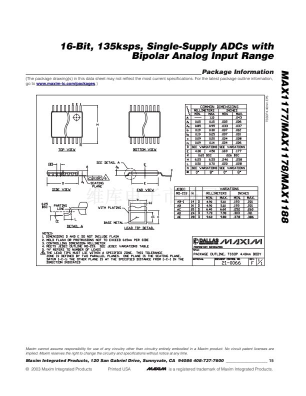
MAX1177/MAX1178/MAX1188
ACQUISITION
CONVERSION
DATA
OUT
ACQUISITION
CONVERSION
DATA
OUT
CS
CS
R/C
R/C
EOC
REF AND
BUFFER
POWER
EOC
REF AND
BUFFER
POWER
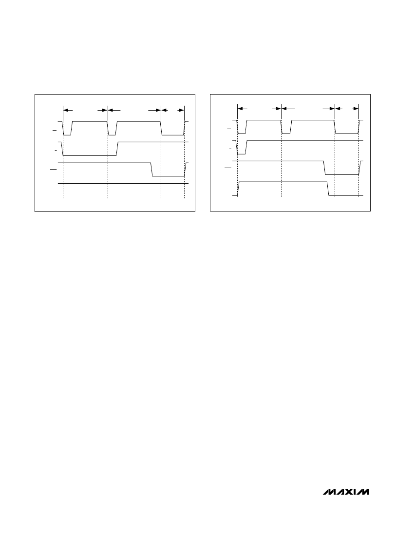
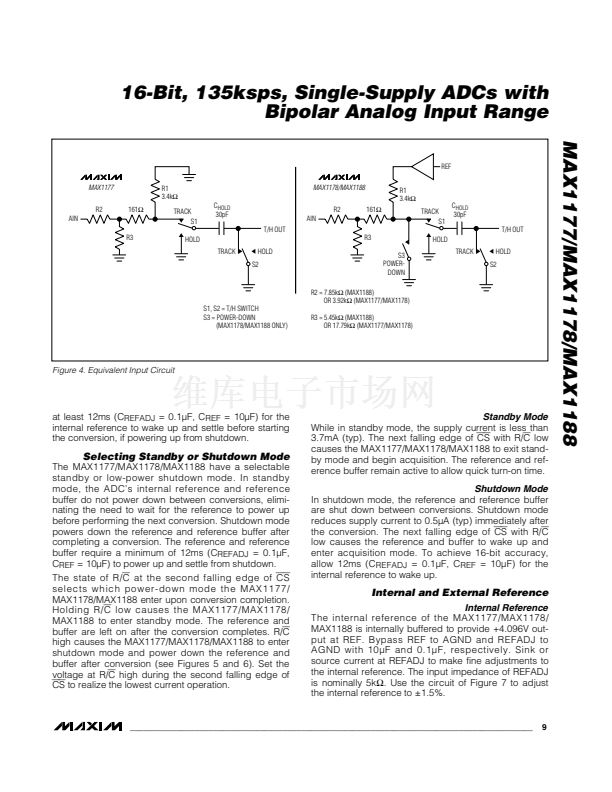
Figure 5. Selecting Standby Mode
Figure 6. Selecting Shutdown Mode
External Reference
An external reference can be placed at either the input
(REFADJ) or the output (REF) of the MAX1177/
MAX1178/MAX1188s鈥?internal buffer amplifier. Using
the buffered REFADJ input makes buffering the exter-
nal reference unnecessary. The input impedance of
REFADJ is typically 5k鈩? The internal buffer output
must be bypassed at REF with a 10碌F capacitor.
Connect REFADJ to AV
DD
to disable the internal buffer.
Directly drive REF using an external 3.8V to 4.2V refer-
ence. During conversion, the external reference must
be able to drive 100碌A of DC load current and have an
output impedance of 10鈩?or less.
For optimal performance, buffer the reference through
an op amp and bypass REF with a 10碌F capacitor.
Consider the MAX1177/MAX1178/MAX1188s鈥?equiva-
lent input noise (0.6 LSB) when choosing a reference.
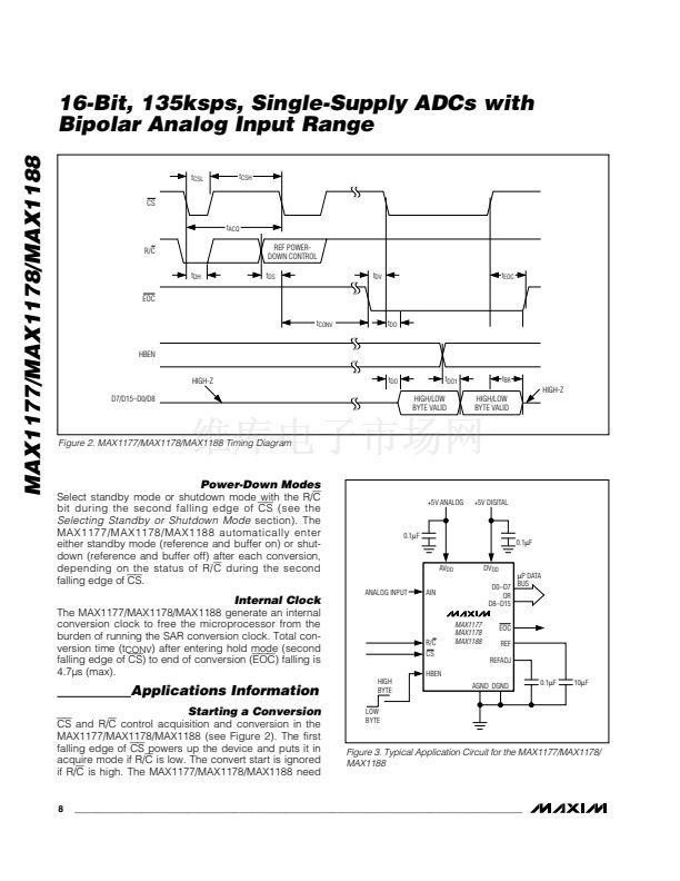
HBEN toggles the output between the high/low byte. The
low byte is loaded onto the output bus when HBEN is low
and the high byte is on the bus when HBEN is high.
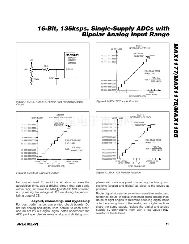
Transfer Function
Figures 8, 9, and 10 show the MAX1177/MAX1178/
MAX1188 output transfer functions. The MAX1188 and
MAX1178 outputs are coded in offset binary, while the
MAX1177 is coded in standard binary.
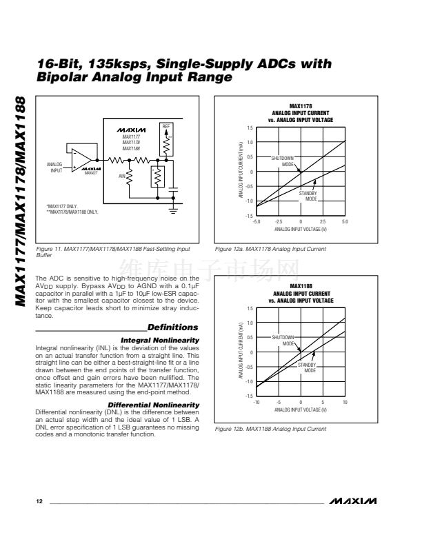
Input Buffer
Most applications require an input buffer amplifier to
achieve 16-bit accuracy and prevent loading the
source. Switch the channels immediately after acquisi-
tion, rather than near the end of, or after, a conversion,
when the input signal is multiplexed. This allows more
time for the input buffer amplifier to respond to a large
step change in input signal. The input amplifier must
have a high enough slew rate to complete the required
output voltage change before the beginning of the
acquisition time. Figure 11 shows an example of this
circuit using the MAX427.
Figures 12a and 12b show how the MAX1188 and
MAX1178 analog input current varies depending on
whether the chip is operating or powered down. The
part is fully powered down between conversions if the
voltage at R/C is set high during the second falling
edge of
CS.
The input current abruptly steps to the
powered-up value at the start of acquisition. This step
in the input current can disrupt the ADC input, depend-
ing on the driving circuit鈥檚 output impedance at high
frequencies. If the driving circuit cannot fully settle by
the end of acquisition, the accuracy of the system can
Reading the Conversion Result
EOC
is provided to flag the microprocessor when a
conversion is complete. The falling edge of
EOC
sig-
nals that the data is valid and ready to be output to the
bus. D0鈥揇15 are the parallel outputs of the
MAX1177/MAX1178/MAX1188. These three-state out-
puts allow for direct connection to a microcontroller I/O
bus. The outputs remain high impedance during acqui-
sition and conversion. Data is loaded onto the output
bus with the third falling edge of
CS
with R/C high (after
t
DO
). Bringing
CS
high forces the output bus back to
high impedance. The MAX1177/MAX1178/MAX1188
then wait for the next falling edge of
CS
to start the next
conversion cycle (see Figure 2).
10
______________________________________________________________________________________


 1
1
 2
2
 3
3
 4
4
 5
5
 6
6
 7
7
 8
8
 9
9
 10
10
 11
11
 12
12
 13
13
 14
14
 15
15
