DS1685/DS1687 3V/5V Real-Time Clocks
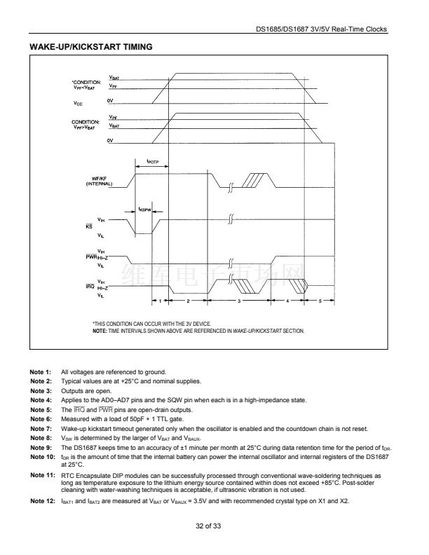
WAKE-UP/KICKSTART TIMING
*THIS CONDITION CAN OCCUR WITH THE 3V DEVICE.
NOTE:
TIME INTERVALS SHOWN ABOVE ARE REFERENCED IN
WAKE-UP/KICKSTART
SECTION.
Note 1:
Note 2:
Note 3:
Note 4:
Note 5:
Note 6:
Note 7:
Note 8:
Note 9:
All voltages are referenced to ground.
Typical values are at +25掳C and nominal supplies.
Outputs are open.
Applies to the AD0鈥揂D7 pins and the SQW pin when each is in a high-impedance state.
The
IRQ
and
PWR
pins are open-drain outputs.
Measured with a load of 50pF + 1 TTL gate.
Wake-up kickstart timeout generated only when the oscillator is enabled and the countdown chain is not reset.
V
SW
is determined by the larger of V
BAT
and V
BAUX
.
The DS1687 keeps time to an accuracy of 卤1 minute per month at 25掳C during data retention time for the period of t
DR
.
Note 10:
t
DR
is the amount of time that the internal battery can power the internal oscillator and internal registers of the DS1687
at 25掳C.
Note 11:
RTC Encapsulate DIP modules can be successfully processed through conventional wave-soldering techniques as
long as temperature exposure to the lithium energy source contained within does not exceed +85掳C. Post-solder
cleaning with water-washing techniques is acceptable, if ultrasonic vibration is not used.
Note 12:
I
BAT1
and I
BAT2
are measured at V
BAT
or V
BAUX
= 3.5V and with recommended crystal type on X1 and X2.
32 of 33


 1
1
 2
2
 3
3
 4
4
 5
5
 6
6
 7
7
 8
8
 9
9
 10
10
 11
11
 12
12
 13
13
 14
14
 15
15
 16
16
 17
17
 18
18
 19
19
 20
20
 21
21
 22
22
 23
23
 24
24
 25
25
 26
26
 27
27
 28
28
 29
29
 30
30
 31
31
 32
32
 33
33
