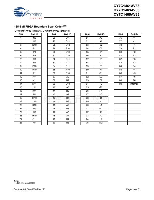
CY7C1461AV33
CY7C1463AV33
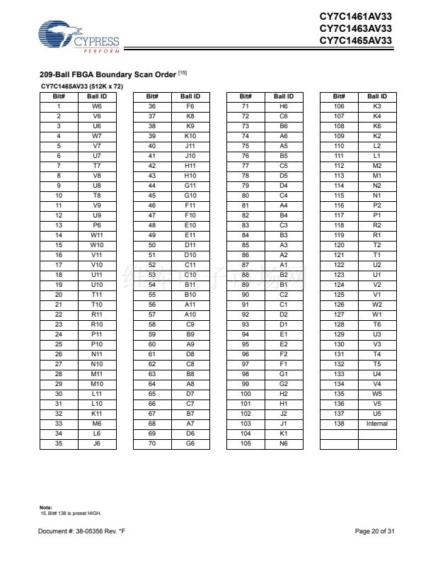
CY7C1465AV33
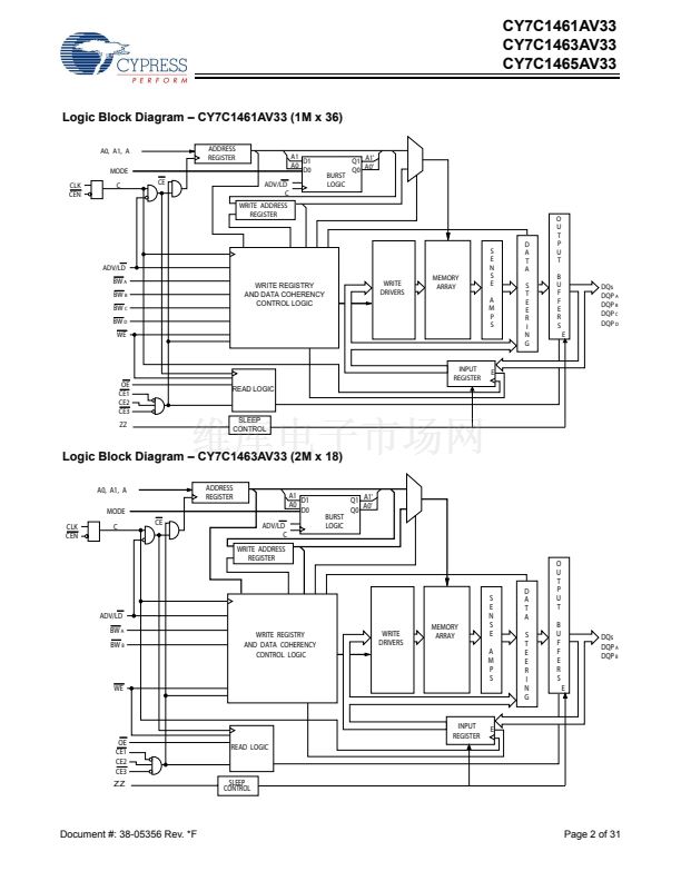
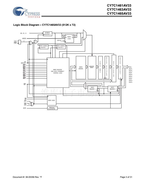
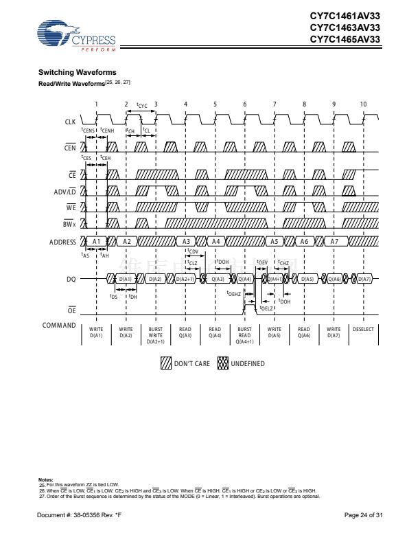
Single Write Accesses
Write access are initiated when the following conditions are
satisfied at clock rise: (1) CEN is asserted LOW, (2) CE
1
, CE
2
,
and CE
3
are ALL asserted active, and (3) the write signal WE
is asserted LOW. The address presented to the address bus
is loaded into the Address Register. The write signals are
latched into the Control Logic block. The data lines are
automatically tri-stated regardless of the state of the OE input
signal. This allows the external logic to present the data on
DQs and DQP
X
.
On the next clock rise the data presented to DQs and DQP
X
(or a subset for byte write operations, see truth table for
details) inputs is latched into the device and the write is
complete. Additional accesses (Read/Write/Deselect) can be
initiated on this cycle.
The data written during the Write operation is controlled by
BW
X
signals. The CY7C1461AV33/CY7C1463AV33/CY7C1465AV33
provides byte write capability that is described in the truth
table. Asserting the Write Enable input (WE) with the selected
Byte Write Select input selectively writes to only the desired
bytes. Bytes not selected during a byte write operation
remains unaltered. A synchronous self timed write mechanism
has been provided to simplify the write operations. Byte write
capability has been included to greatly simplify
Read/Modify/Write sequences, which can be reduced to
simple byte write operations.
Because the CY7C1461AV33/CY7C1463AV33/CY7C1465AV33
is a common IO device, data must not be driven into the device
while the outputs are active. The Output Enable (OE) can be
deasserted HIGH before presenting data to the DQs and
DQP
X
inputs. Doing so tri-states the output drivers. As a safety
precaution, DQs and DQP
X
are automatically tri-stated during
the data portion of a write cycle, regardless of the state of OE.
Burst Write Accesses
The CY7C1461AV33/CY7C1463AV33/CY7C1465AV33 has
an on-chip burst counter that allows the user the ability to
supply a single address and conduct up to four Write opera-
tions without reasserting the address inputs. ADV/LD must be
driven LOW to load the initial address, as described in the
Single Write Access section above. When ADV/LD is driven
HIGH on the subsequent clock rise, the Chip Enables (CE
1
,
CE
2
, and CE
3
) and WE inputs are ignored and the burst
counter is incremented. The correct BW
X
inputs must be
driven in each cycle of the burst write, to write the correct bytes
of data.
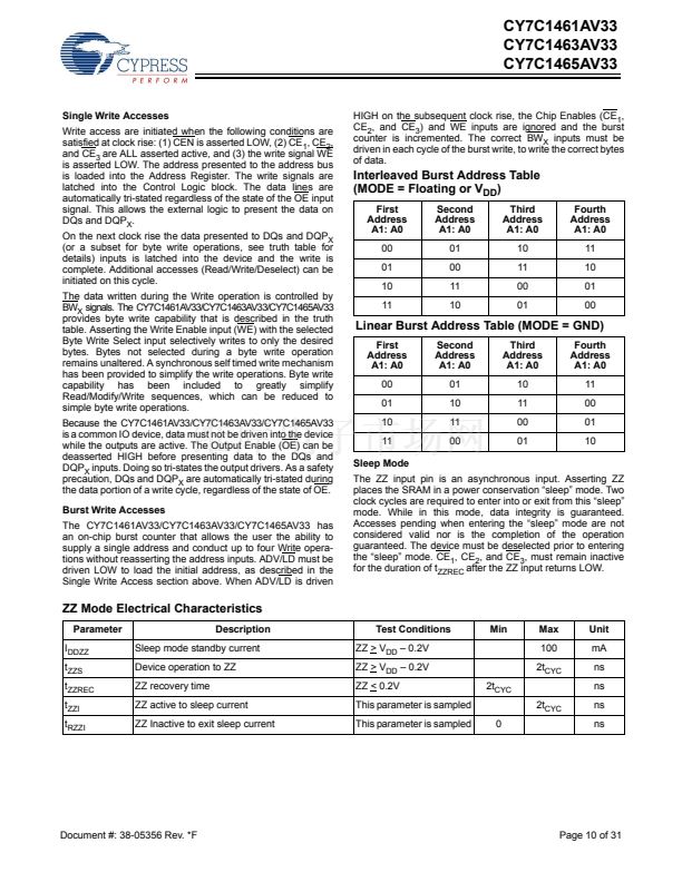
Interleaved Burst Address Table
(MODE = Floating or V
DD
)
.
First
Address
A1: A0
00
01
10
11
Second
Address
A1: A0
01
00
11
10
Third
Address
A1: A0
10
11
00
01
Fourth
Address
A1: A0
11
10
01
00
Linear Burst Address Table (MODE = GND)
First
Address
A1: A0
00
01
10
11
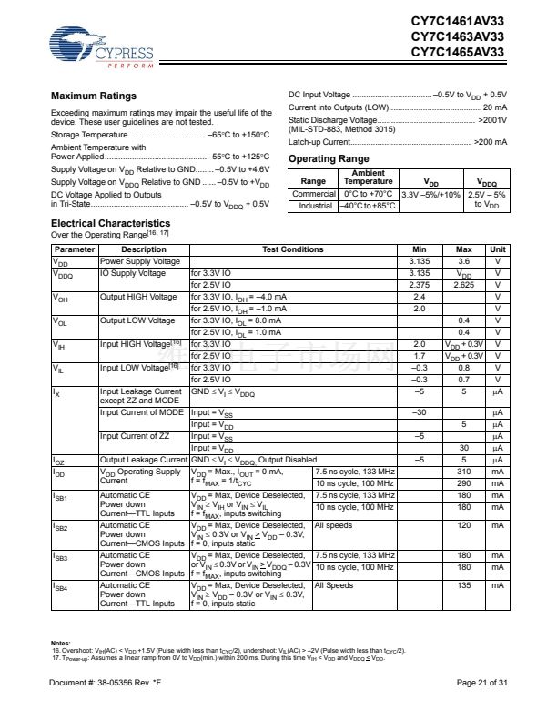
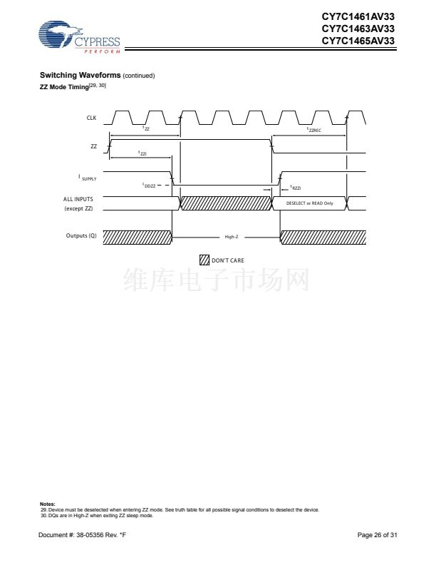
Sleep Mode
The ZZ input pin is an asynchronous input. Asserting ZZ
places the SRAM in a power conservation 鈥渟leep鈥?mode. Two
clock cycles are required to enter into or exit from this 鈥渟leep鈥?/div>
mode. While in this mode, data integrity is guaranteed.
Accesses pending when entering the 鈥渟leep鈥?mode are not
considered valid nor is the completion of the operation
guaranteed. The device must be deselected prior to entering
the 鈥渟leep鈥?mode. CE
1
, CE
2
, and CE
3
, must remain inactive
for the duration of t
ZZREC
after the ZZ input returns LOW.
Second
Address
A1: A0
01
10
11
00
Third
Address
A1: A0
10
11
00
01
Fourth
Address
A1: A0
11
00
01
10
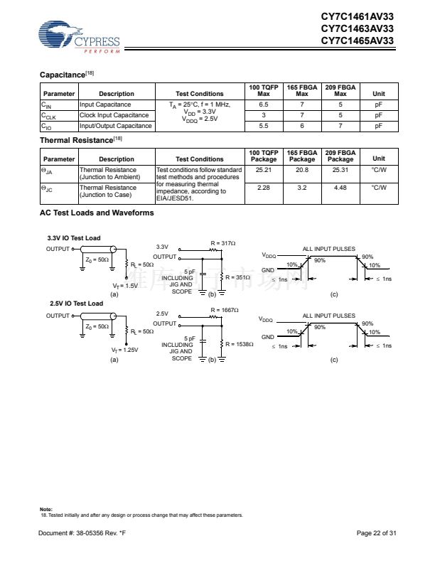
ZZ Mode Electrical Characteristics
Parameter
I
DDZZ
t
ZZS
t
ZZREC
t
ZZI
t
RZZI
Description
Sleep mode standby current
Device operation to ZZ
ZZ recovery time
ZZ active to sleep current
ZZ Inactive to exit sleep current
Test Conditions
ZZ > V
DD
鈥?0.2V
ZZ > V
DD
鈥?0.2V
ZZ < 0.2V
This parameter is sampled
This parameter is sampled
0
2t
CYC
2t
CYC
Min
Max
100
2t
CYC
Unit
mA
ns
ns
ns
ns
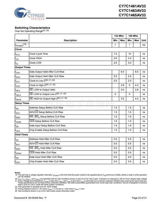
Document #: 38-05356 Rev. *F
Page 10 of 31


 1
1
 2
2
 3
3
 4
4
 5
5
 6
6
 7
7
 8
8
 9
9
 10
10
 11
11
 12
12
 13
13
 14
14
 15
15
 16
16
 17
17
 18
18
 19
19
 20
20
 21
21
 22
22
 23
23
 24
24
 25
25
 26
26
 27
27
 28
28
 29
29
 30
30
 31
31
