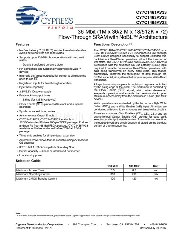
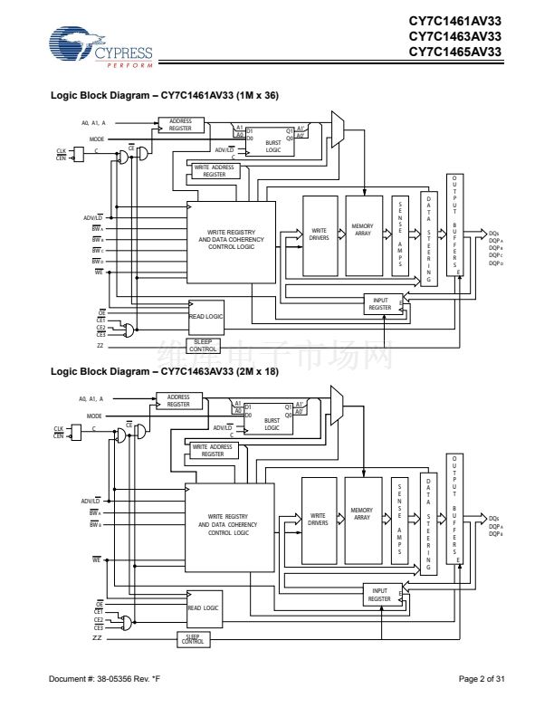
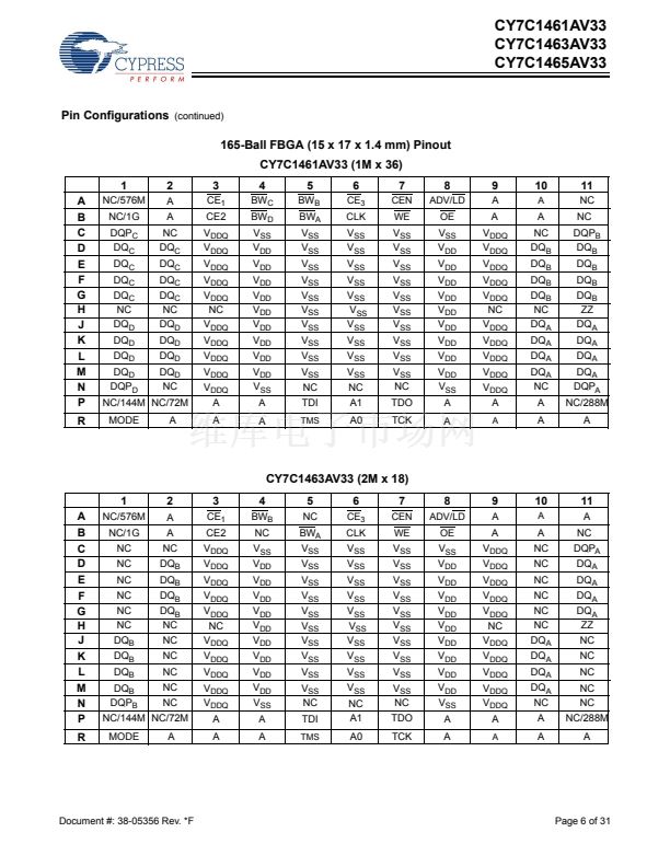
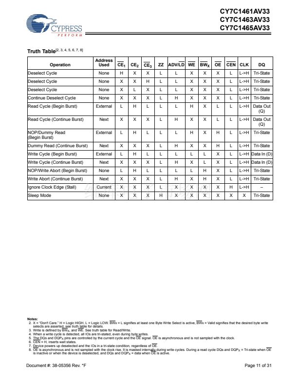
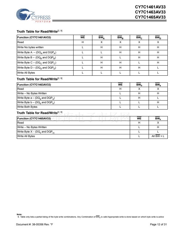
CY7C1461AV33
CY7C1463AV33
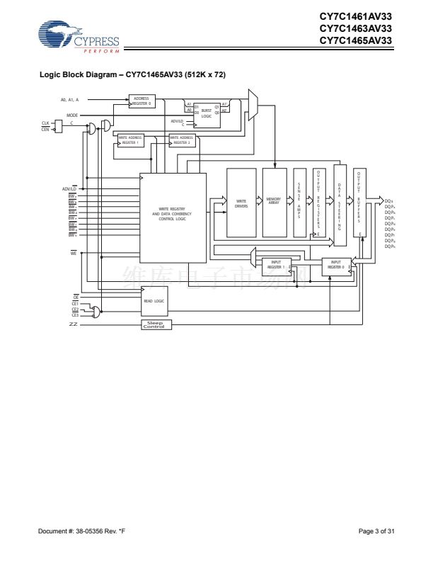
CY7C1465AV33
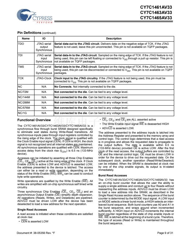
IEEE 1149.1 Serial Boundary Scan (JTAG)
The CY7C1461AV33/CY7C1463AV33/CY7C1465AV33 incor-
porates a serial boundary scan test access port (TAP). This
part is fully compliant with 1149.1. The TAP operates using
JEDEC-standard 3.3V/2.5V IO logic level.
The CY7C1461AV33/CY7C1463AV33/CY7C1465AV33 contains
a TAP controller, instruction register, boundary scan register,
bypass register, and ID register.
Disabling the JTAG Feature
It is possible to operate the SRAM without using the JTAG
feature. To disable the TAP controller, TCK must be tied LOW
(V
SS
) to prevent clocking of the device. TDI and TMS are inter-
nally pulled up and may be unconnected. They may alternately
be connected to V
DD
through a pull up resistor. TDO must be
left unconnected. Upon power up, the device is up in a reset
state which does not interfere with the operation of the device.
Test Data In (TDI)
The TDI ball is used to serially input information into the
registers and can be connected to the input of any of the
registers. The register between TDI and TDO is chosen by the
instruction that is loaded into the TAP instruction register. TDI
is internally pulled up and can be unconnected if the TAP is
unused in an application. TDI is connected to the most signif-
icant bit (MSB) of any register. (See Tap Controller Block
Diagram.)
Test Data Out (TDO)
The TDO output ball is used to serially clock data-out from the
registers. The output is active depending upon the current
state of the TAP state machine. The output changes on the
falling edge of TCK. TDO is connected to the least significant
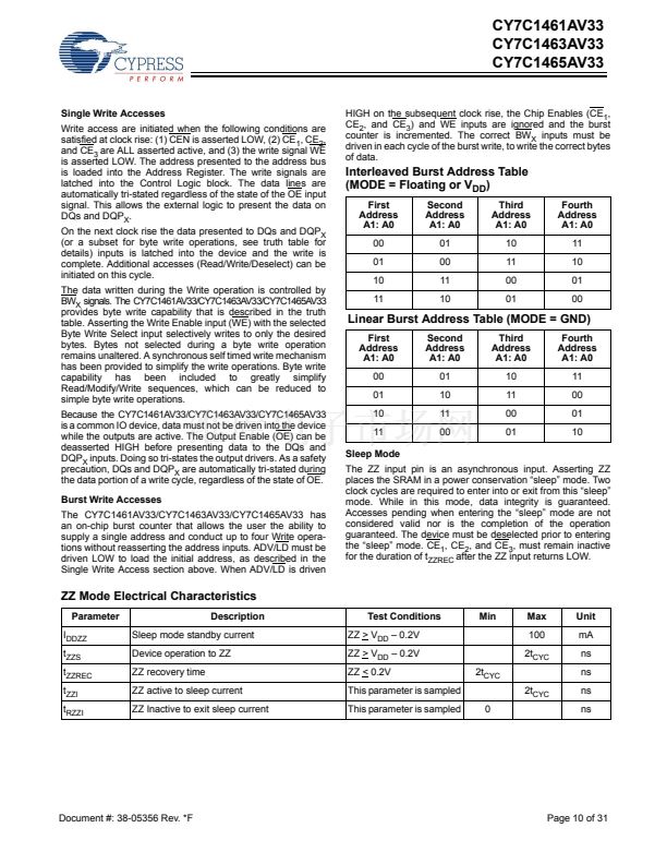
bit (LSB) of any register. (See Tap Controller State Diagram.)
TAP Controller Block Diagram
0
Bypass Register
2 1 0
TAP Controller State Diagram
1
TEST-LOGIC
RESET
0
0
RUN-TEST/
IDLE
1
SELECT
DR-SCAN
0
1
CAPTURE-DR
0
SHIFT-DR
1
EXIT1-DR
0
PAUSE-DR
1
0
EXIT2-DR
1
UPDATE-DR
1
0
0
0
1
0
1
1
SELECT
IR-SCAN
0
CAPTURE-IR
0
SHIFT-IR
1
EXIT1-IR
0
PAUSE-IR
1
EXIT2-IR
1
UPDATE-IR
1
0
0
1
0
1
TDI
Selection
Circuitry
Instruction Register
31 30 29 . . . 2 1 0
Selection
Circuitry
TDO
Identification Register
x . . . . . 2 1 0
Boundary Scan Register
TCK
TMS
TAP CONTROLLER
Performing a TAP Reset
A RESET is performed by forcing TMS HIGH (VDD) for five
rising edges of TCK. This RESET does not affect the operation
of the SRAM and may be performed while the SRAM is
operating.
At power up, the TAP is reset internally to ensure that TDO
comes up in a High-Z state.
The 0/1 next to each state represents the value of TMS at the
rising edge of TCK.
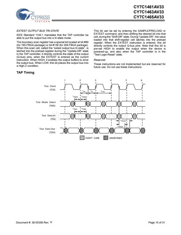
Test Access Port (TAP)
Test Clock (TCK)
The test clock is used only with the TAP controller. All inputs
are captured on the rising edge of TCK. All outputs are driven
from the falling edge of TCK.
Test Mode Select (TMS)
The TMS input is used to give commands to the TAP controller
and is sampled on the rising edge of TCK. It is allowable to
leave this ball unconnected if the TAP is not used. The ball is
pulled up internally, resulting in a logic HIGH level.
TAP Registers
Registers are connected between the TDI and TDO balls and
allow data to be scanned into and out of the SRAM test
circuitry. Only one register can be selected at a time through
the instruction register. Data is serially loaded into the TDI ball
on the rising edge of TCK. Data is output on the TDO ball on
the falling edge of TCK.
Instruction Register
Three-bit instructions can be serially loaded into the instruction
register. This register is loaded when it is placed between the
TDI and TDO balls as shown in the Tap Controller Block
Diagram. Upon power up, the instruction register is loaded
with the IDCODE instruction. It is also loaded with the IDCODE
instruction if the controller is placed in a reset state as
described in the previous section.
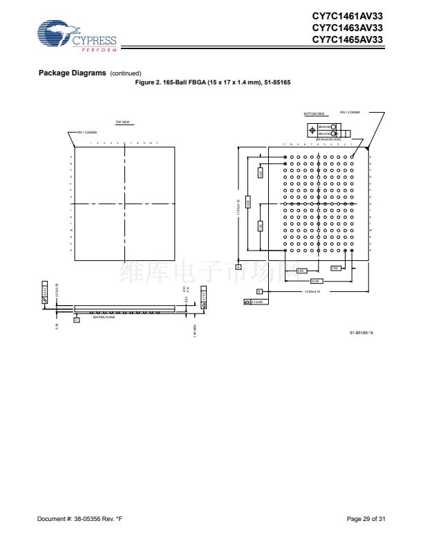
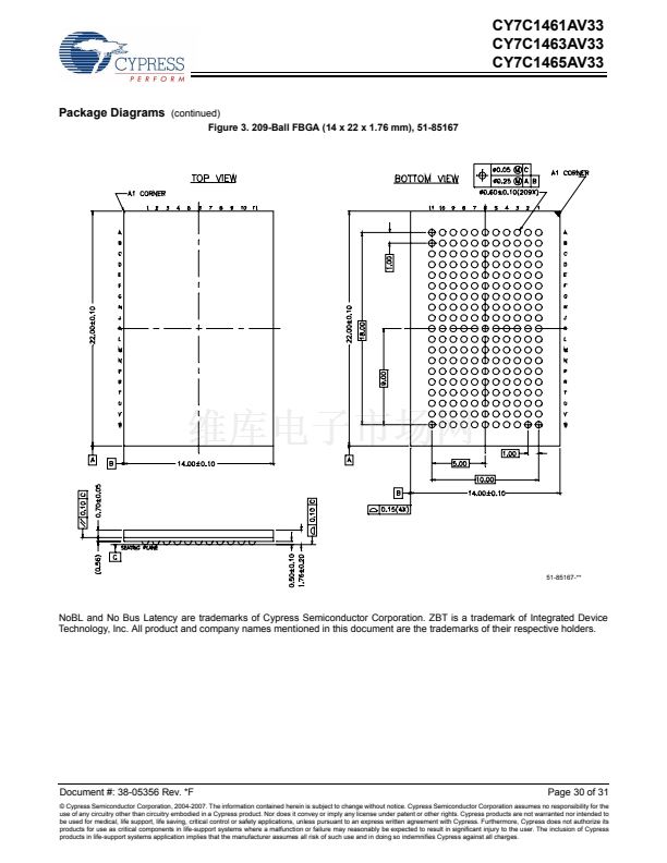
Page 13 of 31
Document #: 38-05356 Rev. *F


 1
1
 2
2
 3
3
 4
4
 5
5
 6
6
 7
7
 8
8
 9
9
 10
10
 11
11
 12
12
 13
13
 14
14
 15
15
 16
16
 17
17
 18
18
 19
19
 20
20
 21
21
 22
22
 23
23
 24
24
 25
25
 26
26
 27
27
 28
28
 29
29
 30
30
 31
31
