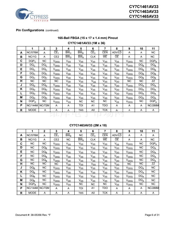
CY7C1461AV33
CY7C1463AV33
CY7C1465AV33
Pin Definitions
Name
A
0
, A
1
, A
BW
A
, BW
B
BW
C
, BW
D
,
BW
E
, BW
F
,
BW
G
, BW
H
WE
ADV/LD
IO
Description
Input-
Address Inputs used to select one of the address locations.
Sampled at the rising edge of the
Synchronous CLK. A
[1:0]
are fed to the two-bit burst counter.
Input-
Byte Write Inputs, Active LOW.
Qualified with WE to conduct writes to the SRAM. Sampled on
Synchronous the rising edge of CLK.
Input-
Write Enable Input, Active LOW.
Sampled on the rising edge of CLK if CEN is active LOW. This
Synchronous signal must be asserted LOW to initiate a write sequence.
Input-
Advance/Load Input.
Used to advance the on-chip address counter or load a new address. When
Synchronous HIGH (and CEN is asserted LOW) the internal burst counter is advanced. When LOW, a new
address can be loaded into the device for an access. After being deselected, ADV/LD must be
driven LOW to load a new address.
Input-
Clock
Clock Input.
Used to capture all synchronous inputs to the device. CLK is qualified with CEN. CLK
is only recognized if CEN is active LOW.
CLK
CE1
CE
2
CE
3
OE
Input-
Chip Enable 1 Input, Active LOW.
Sampled on the rising edge of CLK. Used in conjunction with
Synchronous CE
2
and CE
3
to select/deselect the device.
Input-
Chip Enable 2 Input, Active HIGH.
Sampled on the rising edge of CLK. Used in conjunction with
Synchronous CE
1
and CE
3
to select/deselect the device.
Input-
Chip Enable 3 Input, Active LOW.
Sampled on the rising edge of CLK. Used in conjunction with
Synchronous CE
1
and CE
2
to select/deselect the device.
Input-
Output Enable, asynchronous input, Active LOW.
Combined with the synchronous logic block
Asynchronous inside the device to control the direction of the IO pins. When LOW, the IO pins are allowed to
behave as outputs. When deasserted HIGH, IO pins are tri-stated, and act as input data pins. OE
is masked during the data portion of a write sequence, during the first clock when emerging from
a deselected state, when the device is deselected.
Input-
Clock Enable Input, Active LOW.
When asserted LOW the Clock signal is recognized by the
Synchronous SRAM. When deasserted HIGH the Clock signal is masked. Since deasserting CEN does not
deselect the device, use CEN to extend the previous cycle when required.
Input-
ZZ 鈥淪leep鈥?Input.
This active HIGH input places the device in a non-time critical 鈥渟leep鈥?condition
Asynchronous with data integrity preserved. During normal operation, this pin has to be LOW or left floating. ZZ
pin has an internal pull down.
IO-
Bidirectional Data IO lines.
As inputs, they feed into an on-chip data register that is triggered by
Synchronous the rising edge of CLK. As outputs, they deliver the data contained in the memory location specified
by the addresses presented during the previous clock rise of the read cycle. The direction of the
pins is controlled by OE. When OE is asserted LOW, the pins behave as outputs. When HIGH,
DQ
s
and DQP
[A:D]
are placed in a tri-state condition.The outputs are automatically tri-stated during
the data portion of a write sequence, during the first clock when emerging from a deselected state,
and when the device is deselected, regardless of the state of OE.
IO-
Bidirectional Data Parity IO Lines.
Functionally, these signals are identical to DQ
s
. During write
Synchronous sequences, DQP
X
is controlled by BW
X
correspondingly.
Input Strap Pin
Mode Input. Selects the burst order of the device.
When tied to Gnd selects linear burst sequence. When tied to V
DD
or left floating selects interleaved
burst sequence.
Power Supply
Power supply inputs to the core of the device.
IO Power
Supply
Ground
Power supply for the IO circuitry.
Ground for the device.
CEN
ZZ
DQ
s
DQP
X
MODE
V
DD
V
DDQ
V
SS
Document #: 38-05356 Rev. *F
Page 8 of 31


 1
1
 2
2
 3
3
 4
4
 5
5
 6
6
 7
7
 8
8
 9
9
 10
10
 11
11
 12
12
 13
13
 14
14
 15
15
 16
16
 17
17
 18
18
 19
19
 20
20
 21
21
 22
22
 23
23
 24
24
 25
25
 26
26
 27
27
 28
28
 29
29
 30
30
 31
31
