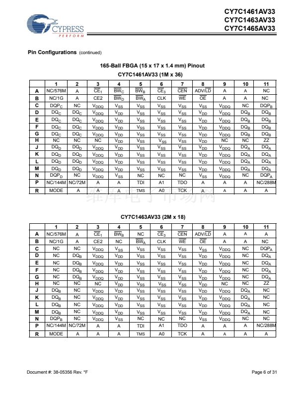
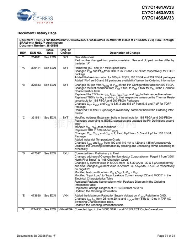
CY7C1461AV33
CY7C1463AV33
CY7C1465AV33
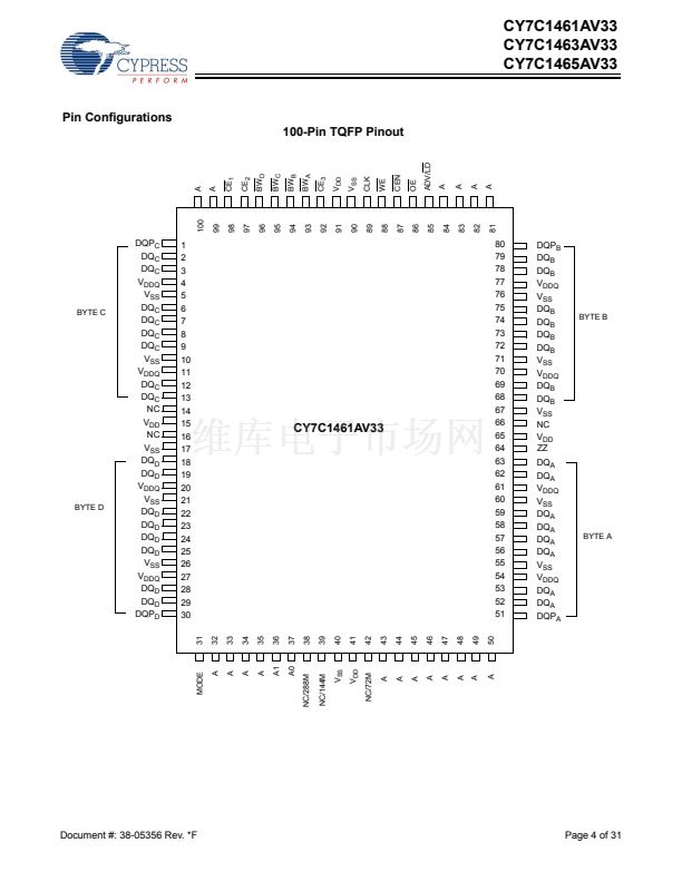
Pin Definitions
(continued)
Name
TDO
IO
Description
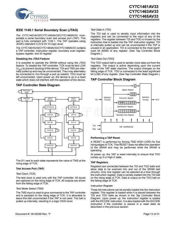
JTAG serial
Serial data-out to the JTAG circuit.
Delivers data on the negative edge of TCK. If the JTAG
feature is not used, leave this pin unconnected. This pin is not available on TQFP packages.
output
Synchronous
JTAG serial
Serial data-In to the JTAG circuit.
Sampled on the rising edge of TCK. If the JTAG feature is not
being used, this pin can be left floating or connected to V
DD
through a pull up resistor. This pin is
input
Synchronous not available on TQFP packages.
JTAG serial
Serial data-In to the JTAG circuit.
Sampled on the rising edge of TCK. If the JTAG feature is not
input
being used, this pin can be disconnected or connected to V
DD
. This pin is not available on TQFP
Synchronous packages.
JTAG-Clock
N/A
N/A
N/A
N/A
N/A
N/A
Clock input to the JTAG circuitry.
If the JTAG feature is not being used, this pin must be
connected to V
SS
. This pin is not available on TQFP packages.
No Connects.
Not internally connected to the die.
Not connected to the die.
Can be tied to any voltage level.
Not connected to the die.
Can be tied to any voltage level.
Not connected to the die.
Can be tied to any voltage level.
Not connected to the die.
Can be tied to any voltage level.
Not connected to the die.
Can be tied to any voltage level.
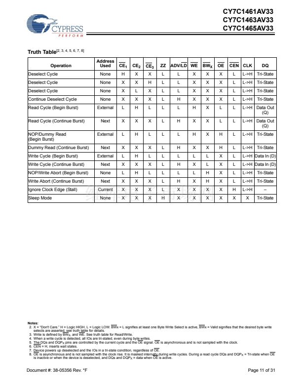
鈥?CE
1
, CE
2
, and CE
3
are ALL asserted active
鈥?The Write Enable input signal WE is deasserted HIGH
鈥?ADV/LD is asserted LOW.
The address presented to the address inputs is latched into
the Address Register and presented to the memory array and
control logic. The control logic determines that a read access
is in progress and allows the requested data to propagate to
the output buffers. The data is available within 6.5 ns
(133-MHz device) provided OE is active LOW. After the first
clock of the read access, the output buffers are controlled by
OE and the internal control logic. OE must be driven LOW in
order for the device to drive out the requested data. On the
subsequent clock, another operation (Read/Write/Deselect)
can be initiated. When the SRAM is deselected at clock rise
by one of the chip enable signals, its output is tri-stated
immediately.
Burst Read Accesses
The CY7C1461AV33/CY7C1463AV33/CY7C1465AV33 has
an on-chip burst counter that allows the user the ability to
supply a single address and conduct up to four Reads without
reasserting the address inputs. ADV/LD must be driven LOW
to load a new address into the SRAM, as described in the
Single Read Access section above. The sequence of the burst
counter is determined by the MODE input signal. A LOW input
on MODE selects a linear burst mode, a HIGH selects an inter-
leaved burst sequence. Both burst counters use A0 and A1 in
the burst sequence, and wraps around when incremented
sufficiently. A HIGH input on ADV/LD increments the internal
burst counter regardless of the state of chip enable inputs or
WE. WE is latched at the beginning of a burst cycle. Therefore,
the type of access (Read or Write) is maintained throughout
the burst sequence.
Page 9 of 31
TDI
TMS
TCK
NC
NC/72M
NC/144M
NC/288M
NC/576M
NC/1G
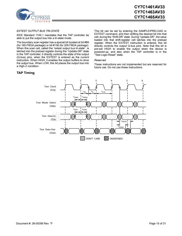
Functional Overview
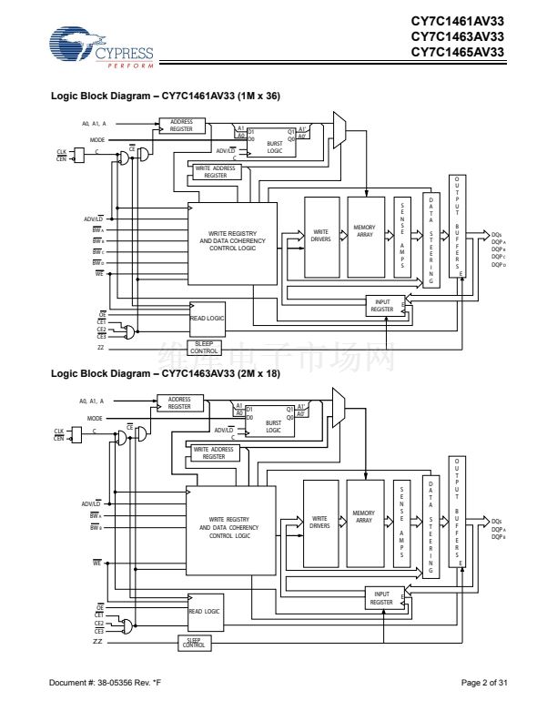
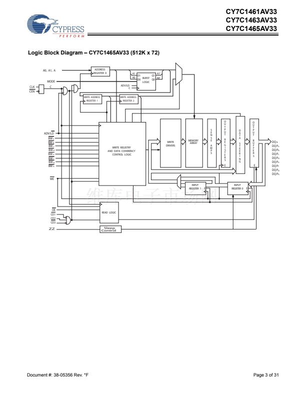
The CY7C1461AV33/CY7C1463AV33/CY7C1465AV33 is a
synchronous flow through burst SRAM designed specifically
to eliminate wait states during Write-Read transitions. All
synchronous inputs pass through input registers controlled by
the rising edge of the clock. The clock signal is qualified with
the Clock Enable input signal (CEN). If CEN is HIGH, the clock
signal is not recognized and all internal states are maintained.
All synchronous operations are qualified with CEN. Maximum
access delay from the clock rise (t
CDV
) is 6.5 ns (133-MHz
device).
Accesses can be initiated by asserting all three Chip Enables
(CE
1
, CE
2
, CE
3
) active at the rising edge of the clock. If Clock
Enable (CEN) is active LOW and ADV/LD is asserted LOW,
the address presented to the device is latched. The access
can either be a read or write operation, depending on the
status of the Write Enable (WE). BW
X
can be used to conduct
byte write operations.
Write operations are qualified by the Write Enable (WE). All
writes are simplified with on-chip synchronous self timed write
circuitry.
Three synchronous Chip Enables (CE
1
, CE
2
, CE
3
) and an
asynchronous Output Enable (OE) simplify depth expansion.
All operations (Reads, Writes, and Deselects) are pipelined.
ADV/LD must be driven LOW after the device has been
deselected to load a new address for the next operation.
Single Read Accesses
A read access is initiated when these conditions are satisfied
at clock rise:
鈥?CEN is asserted LOW
Document #: 38-05356 Rev. *F


 1
1
 2
2
 3
3
 4
4
 5
5
 6
6
 7
7
 8
8
 9
9
 10
10
 11
11
 12
12
 13
13
 14
14
 15
15
 16
16
 17
17
 18
18
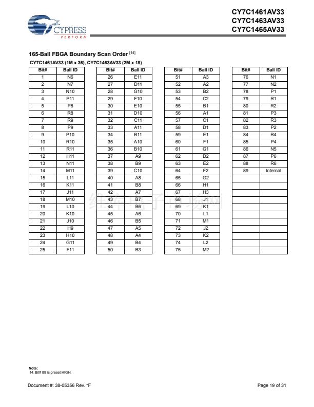 19
19
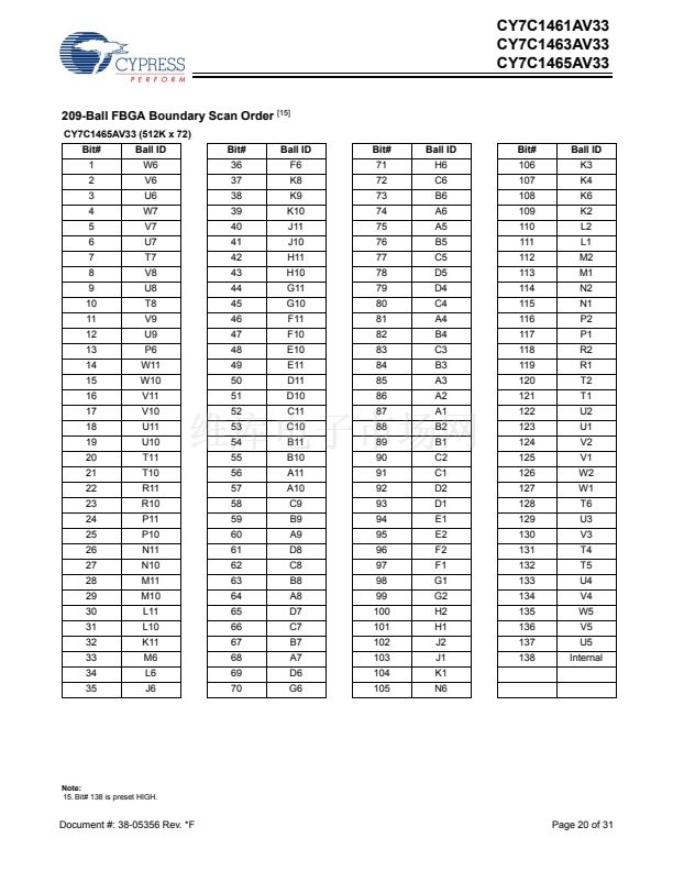 20
20
 21
21
 22
22
 23
23
 24
24
 25
25
 26
26
 27
27
 28
28
 29
29
 30
30
 31
31
