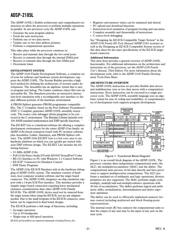
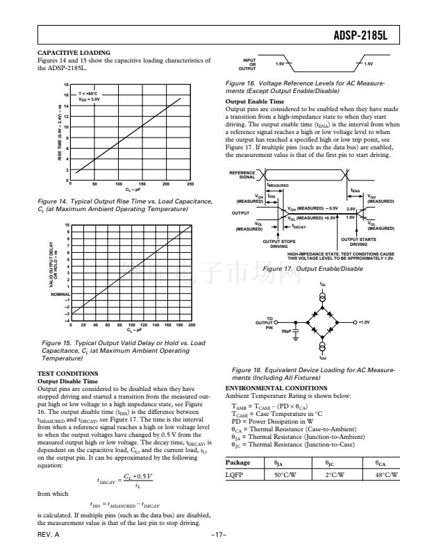
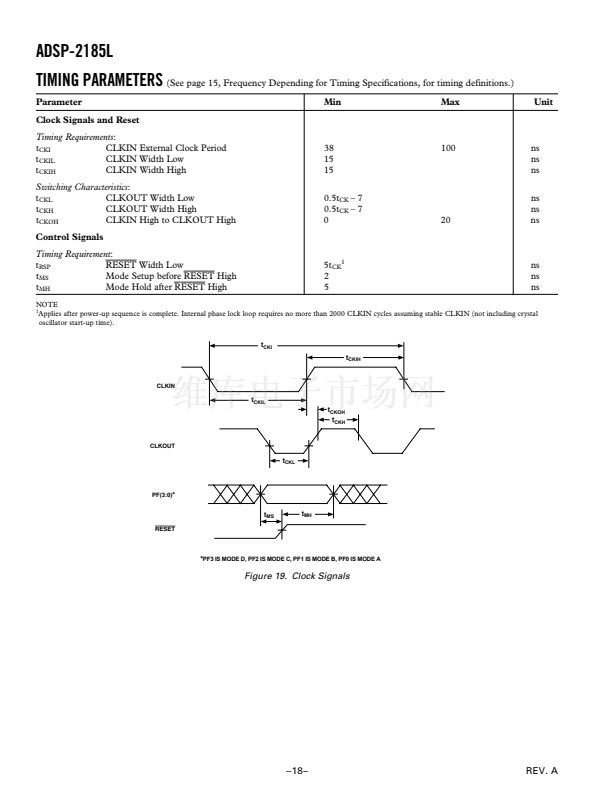
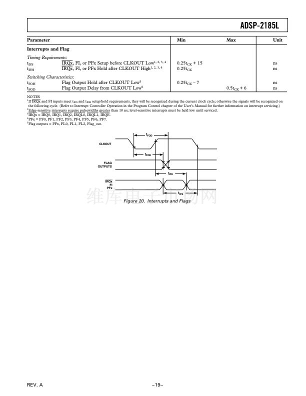
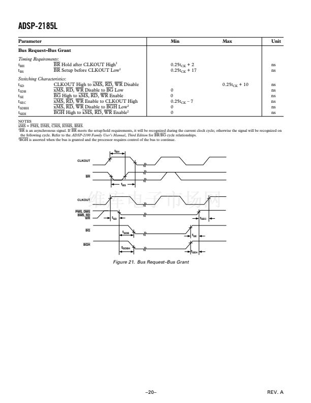
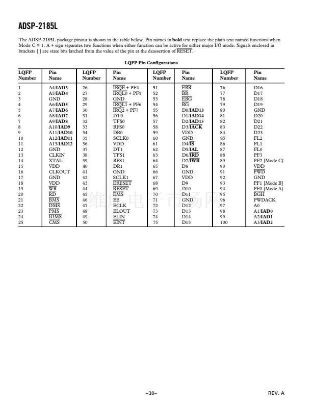
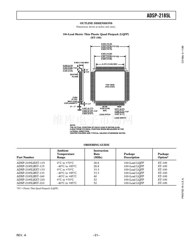
ADSP-2185L
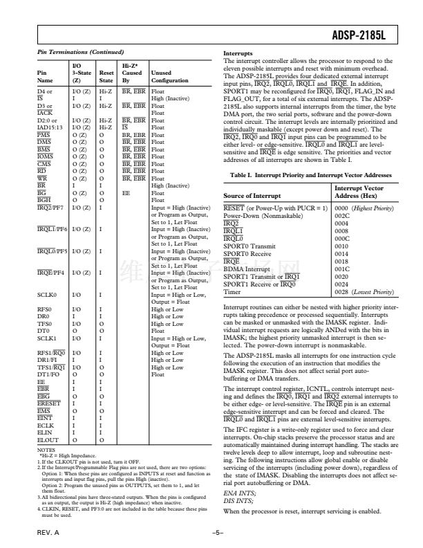
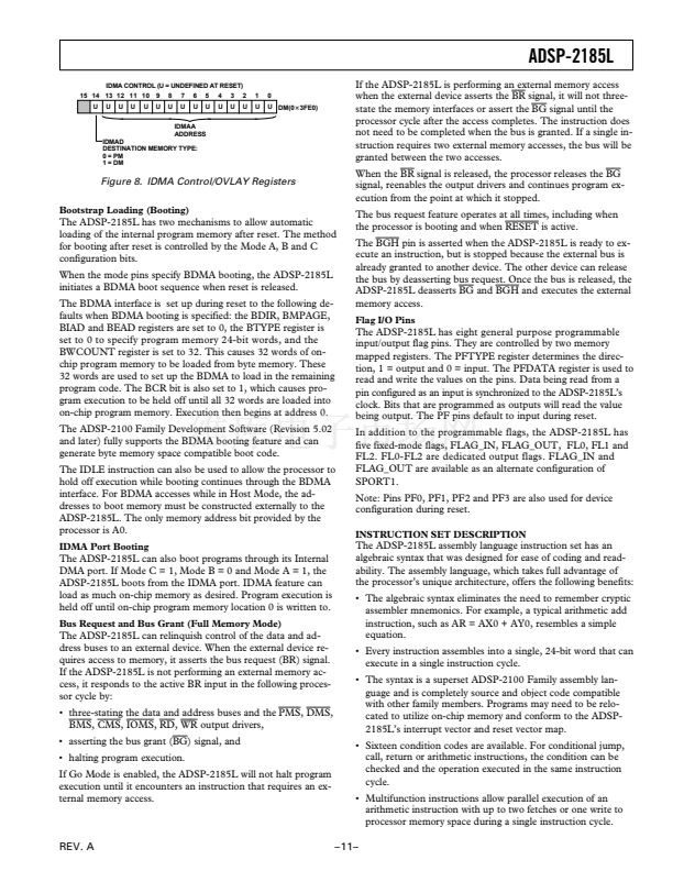
IDMA CONTROL (U = UNDEFINED AT RESET)
15 14 13 12 11 10
U
U
U
U
U
9
U
8
U
7
U
6
U
5
U
4
U
3
U
2
U
1
U
0
U DM(0 3FE0)
IDMAA
ADDRESS
IDMAD
DESTINATION MEMORY TYPE:
0 = PM
1 = DM
If the ADSP-2185L is performing an external memory access
when the external device asserts the
BR
signal, it will not three-
state the memory interfaces or assert the
BG
signal until the
processor cycle after the access completes. The instruction does
not need to be completed when the bus is granted. If a single in-
struction requires two external memory accesses, the bus will be
granted between the two accesses.
When the
BR
signal is released, the processor releases the
BG
signal, reenables the output drivers and continues program ex-
ecution from the point at which it stopped.
The bus request feature operates at all times, including when
the processor is booting and when
RESET
is active.
The
BGH
pin is asserted when the ADSP-2185L is ready to ex-
ecute an instruction, but is stopped because the external bus is
already granted to another device. The other device can release
the bus by deasserting bus request. Once the bus is released, the
ADSP-2185L deasserts
BG
and
BGH
and executes the external
memory access.
Flag I/O Pins
Figure 8. IDMA Control/OVLAY Registers
Bootstrap Loading (Booting)
The ADSP-2185L has two mechanisms to allow automatic
loading of the internal program memory after reset. The method
for booting after reset is controlled by the Mode A, B and C
configuration bits.
When the mode pins specify BDMA booting, the ADSP-2185L
initiates a BDMA boot sequence when reset is released.
The BDMA interface is set up during reset to the following de-
faults when BDMA booting is specified: the BDIR, BMPAGE,
BIAD and BEAD registers are set to 0, the BTYPE register is
set to 0 to specify program memory 24-bit words, and the
BWCOUNT register is set to 32. This causes 32 words of on-
chip program memory to be loaded from byte memory. These
32 words are used to set up the BDMA to load in the remaining
program code. The BCR bit is also set to 1, which causes pro-
gram execution to be held off until all 32 words are loaded into
on-chip program memory. Execution then begins at address 0.
The ADSP-2100 Family Development Software (Revision 5.02
and later) fully supports the BDMA booting feature and can
generate byte memory space compatible boot code.
The IDLE instruction can also be used to allow the processor to
hold off execution while booting continues through the BDMA
interface. For BDMA accesses while in Host Mode, the ad-
dresses to boot memory must be constructed externally to the
ADSP-2185L. The only memory address bit provided by the
processor is A0.
IDMA Port Booting
The ADSP-2185L has eight general purpose programmable
input/output flag pins. They are controlled by two memory
mapped registers. The PFTYPE register determines the direc-
tion, 1 = output and 0 = input. The PFDATA register is used to
read and write the values on the pins. Data being read from a
pin configured as an input is synchronized to the ADSP-2185L鈥檚
clock. Bits that are programmed as outputs will read the value
being output. The PF pins default to input during reset.
In addition to the programmable flags, the ADSP-2185L has
five fixed-mode flags, FLAG_IN, FLAG_OUT, FL0, FL1 and
FL2. FL0-FL2 are dedicated output flags. FLAG_IN and
FLAG_OUT are available as an alternate configuration of
SPORT1.
Note: Pins PF0, PF1, PF2 and PF3 are also used for device
configuration during reset.
INSTRUCTION SET DESCRIPTION
The ADSP-2185L can also boot programs through its Internal
DMA port. If Mode C = 1, Mode B = 0 and Mode A = 1, the
ADSP-2185L boots from the IDMA port. IDMA feature can
load as much on-chip memory as desired. Program execution is
held off until on-chip program memory location 0 is written to.
Bus Request and Bus Grant (Full Memory Mode)
The ADSP-2185L assembly language instruction set has an
algebraic syntax that was designed for ease of coding and read-
ability. The assembly language, which takes full advantage of
the processor鈥檚 unique architecture, offers the following benefits:
鈥?The algebraic syntax eliminates the need to remember cryptic
assembler mnemonics. For example, a typical arithmetic add
instruction, such as AR = AX0 + AY0, resembles a simple
equation.
鈥?Every instruction assembles into a single, 24-bit word that can
execute in a single instruction cycle.
鈥?The syntax is a superset ADSP-2100 Family assembly lan-
guage and is completely source and object code compatible
with other family members. Programs may need to be relo-
cated to utilize on-chip memory and conform to the ADSP-
2185L鈥檚 interrupt vector and reset vector map.
鈥?Sixteen condition codes are available. For conditional jump,
call, return or arithmetic instructions, the condition can be
checked and the operation executed in the same instruction
cycle.
鈥?Multifunction instructions allow parallel execution of an
arithmetic instruction with up to two fetches or one write to
processor memory space during a single instruction cycle.
鈥?1鈥?/div>
The ADSP-2185L can relinquish control of the data and ad-
dress buses to an external device. When the external device re-
quires access to memory, it asserts the bus request (BR) signal.
If the ADSP-2185L is not performing an external memory ac-
cess, it responds to the active BR input in the following proces-
sor cycle by:
鈥?three-stating the data and address buses and the
PMS, DMS,
BMS, CMS, IOMS, RD, WR
output drivers,
鈥?asserting the bus grant (BG) signal, and
鈥?halting program execution.
If Go Mode is enabled, the ADSP-2185L will not halt program
execution until it encounters an instruction that requires an ex-
ternal memory access.
REV. A


 1
1
 2
2
 3
3
 4
4
 5
5
 6
6
 7
7
 8
8
 9
9
 10
10
 11
11
 12
12
 13
13
 14
14
 15
15
 16
16
 17
17
 18
18
 19
19
 20
20
 21
21
 22
22
 23
23
 24
24
 25
25
 26
26
 27
27
 28
28
 29
29
 30
30
 31
31
