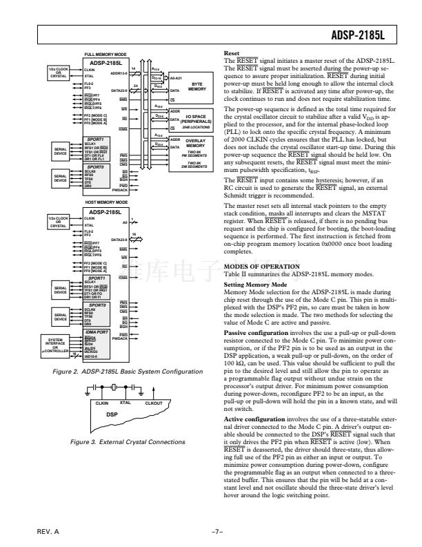
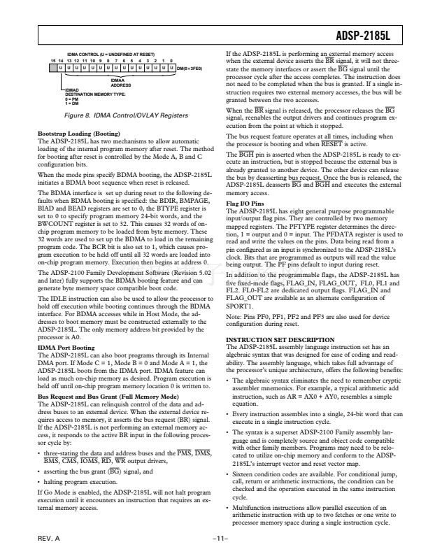
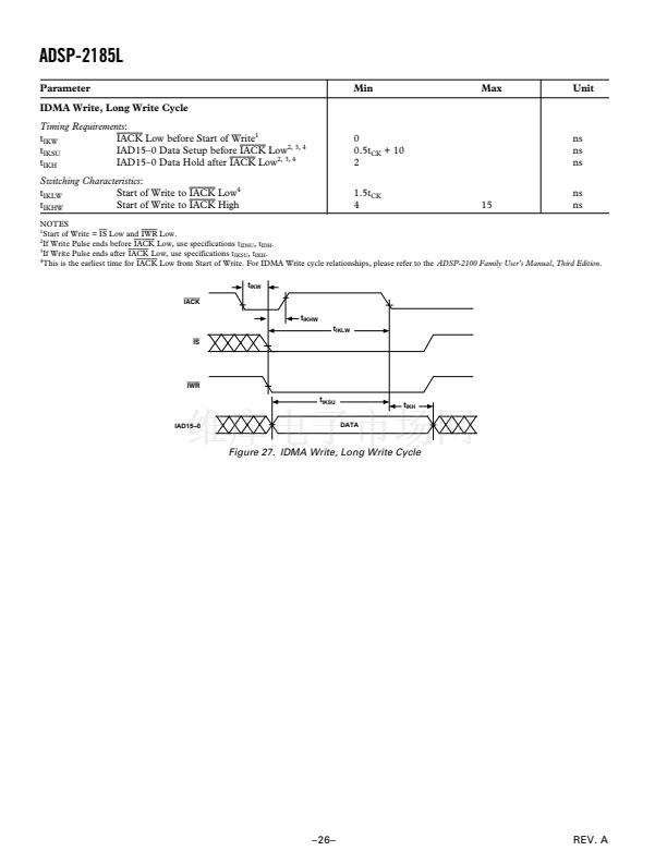
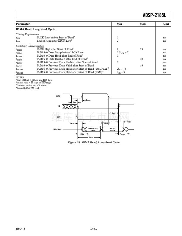
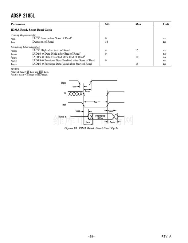
ADSP-2185L
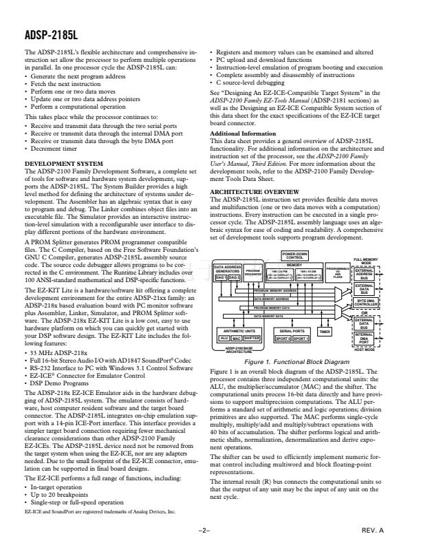
A powerful program sequencer and two dedicated data address
generators ensure efficient delivery of operands to these computa-
tional units. The sequencer supports conditional jumps, subroutine
calls and returns in a single cycle. With internal loop counters and
loop stacks, the ADSP-2185L executes looped code with zero over-
head; no explicit jump instructions are required to maintain loops.
Two data address generators (DAGs) provide addresses for
simultaneous dual operand fetches (from data memory and pro-
gram memory). Each DAG maintains and updates four address
pointers. Whenever the pointer is used to access data (indirect
addressing), it is post-modified by the value of one of four pos-
sible modify registers. A length value may be associated with
each pointer to implement automatic modulo addressing for
circular buffers.
Efficient data transfer is achieved with the use of five internal
buses:
鈥?Program Memory Address (PMA) Bus
鈥?Program Memory Data (PMD) Bus
鈥?Data Memory Address (DMA) Bus
鈥?Data Memory Data (DMD) Bus
鈥?Result (R) Bus
The two address buses (PMA and DMA) share a single external
address bus, allowing memory to be expanded off-chip, and the
two data buses (PMD and DMD) share a single external data
bus. Byte memory space and I/O memory space also share the
external buses.
Program memory can store both instructions and data, permit-
ting the ADSP-2185L to fetch two operands in a single cycle,
one from program memory and one from data memory. The
ADSP-2185L can fetch an operand from program memory and
the next instruction in the same cycle.
In lieu of the address and data bus for external memory connec-
tion, the ADSP-2185L may be configured for 16-bit Internal
DMA port (IDMA port) connection to external systems. The
IDMA port is made up of 16 data/address pins and five control
pins. The IDMA port provides transparent, direct access to the
DSPs on-chip program and data RAM.
An interface to low cost byte-wide memory is provided by the
Byte DMA port (BDMA port). The BDMA port is bidirectional
and can directly address up to four megabytes of external RAM
or ROM for off-chip storage of program overlays or data tables.
The byte memory and I/O memory space interface supports slow
memories and I/O memory-mapped peripherals with program-
mable wait state generation. External devices can gain control of
external buses with bus request/grant signals (BR,
BGH,
and
BG).
One execution mode (Go Mode) allows the ADSP-2185L to con-
tinue running from on-chip memory. Normal execution mode re-
quires the processor to halt while buses are granted.
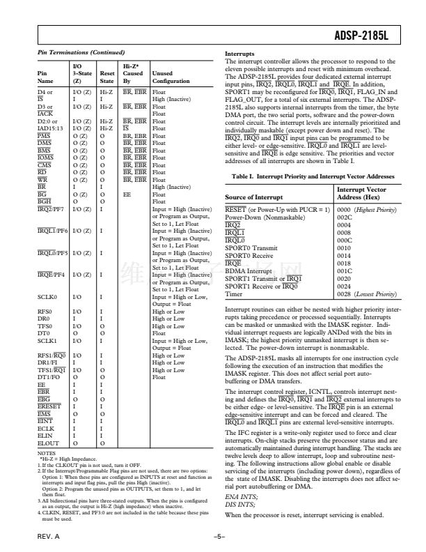
The ADSP-2185L can respond to eleven interrupts. There can
be up to six external interrupts (one edge-sensitive, two level-
sensitive and three configurable) and seven internal interrupts
generated by the timer, the serial ports (SPORTs), the Byte
DMA port and the power-down circuitry. There is also a master
RESET
signal. The two serial ports provide a complete synchro-
nous serial interface with optional companding in hardware and a
wide variety of framed or frameless data transmit and receive
modes of operation.
Each port can generate an internal programmable serial clock or
accept an external serial clock.
REV. A
鈥?鈥?/div>
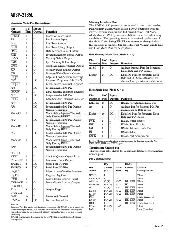
The ADSP-2185L provides up to 13 general-purpose flag pins.
The data input and output pins on SPORT1 can be alternatively
configured as an input flag and an output flag. In addition, there
are eight flags that are programmable as inputs or outputs and
three flags that are always outputs.
A programmable interval timer generates periodic interrupts. A
16-bit count register (TCOUNT) is decremented every
n
pro-
cessor cycle, where
n
is a scaling value stored in an 8-bit register
(TSCALE). When the value of the count register reaches zero,
an interrupt is generated and the count register is reloaded from
a 16-bit period register (TPERIOD).
Serial Ports
The ADSP-2185L incorporates two complete synchronous se-
rial ports (SPORT0 and SPORT1) for serial communications
and multiprocessor communication.
Here is a brief list of the capabilities of the ADSP-2185L
SPORTs. For additional information on Serial Ports, refer to
the
ADSP-2100 Family User鈥檚 Manual, Third Edition.
鈥?SPORTs are bidirectional and have a separate, double-
buffered transmit and receive section.
鈥?SPORTs can use an external serial clock or generate their
own serial clock internally.
鈥?SPORTs have independent framing for the receive and trans-
mit sections. Sections run in a frameless mode or with frame
synchronization signals internally or externally generated.
Frame sync signals are active high or inverted, with either of
two pulsewidths and timings.
鈥?SPORTs support serial data word lengths from 3 to 16 bits
and provide optional A-law and
碌-law
companding according
to CCITT recommendation G.711.
鈥?SPORT receive and transmit sections can generate unique in-
terrupts on completing a data word transfer.
鈥?SPORTs can receive and transmit an entire circular buffer of
data with only one overhead cycle per data word. An interrupt
is generated after a data buffer transfer.
鈥?SPORT0 has a multichannel interface to selectively receive
and transmit a 24- or 32-word, time-division multiplexed,
serial bitstream.
鈥?SPORT1 can be configured to have two external interrupts
(IRQ0 and
IRQ1)
and the Flag In and Flag Out signals. The
internally generated serial clock may still be used in this
configuration.
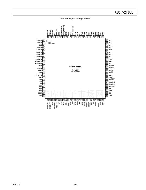
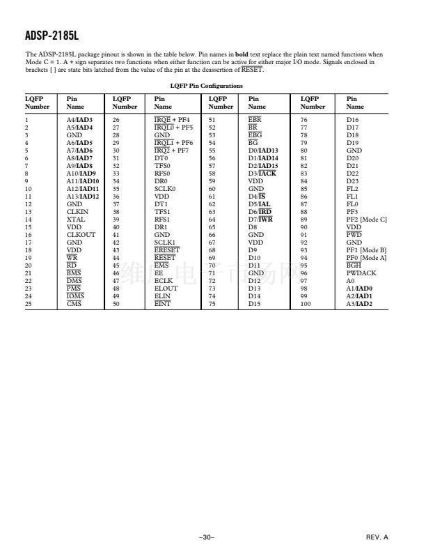
PIN DESCRIPTIONS
The ADSP-2185L is available in a 100-lead LQFP package. In
order to maintain maximum functionality and reduce package
size and pin count, some serial port, programmable flag, inter-
rupt and external bus pins have dual, multiplexed functionality.
The external bus pins are configured during
RESET
only,
while serial port pins are software configurable during program
execution. Flag and interrupt functionality is retained concur-
rently on multiplexed pins. In cases where pin functionality is
reconfigurable, the default state is shown in plain text; alternate
functionality is shown in italics. See Common-Mode Pin
Descriptions.


 1
1
 2
2
 3
3
 4
4
 5
5
 6
6
 7
7
 8
8
 9
9
 10
10
 11
11
 12
12
 13
13
 14
14
 15
15
 16
16
 17
17
 18
18
 19
19
 20
20
 21
21
 22
22
 23
23
 24
24
 25
25
 26
26
 27
27
 28
28
 29
29
 30
30
 31
31
