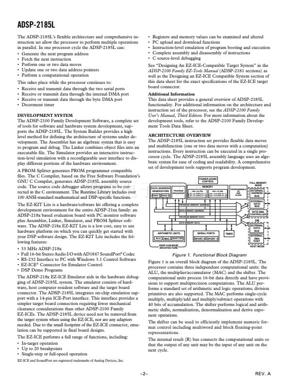
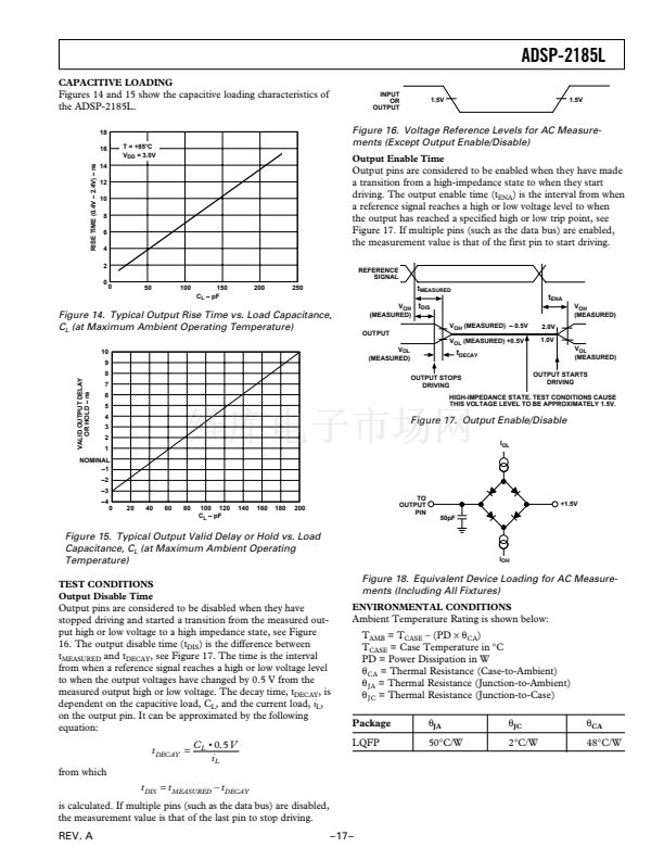
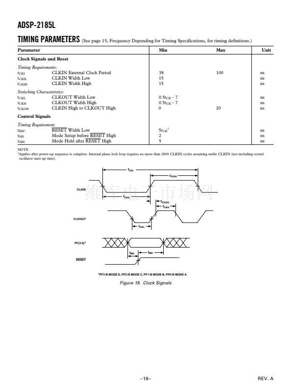
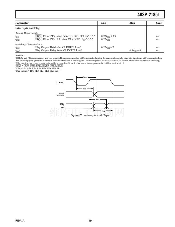
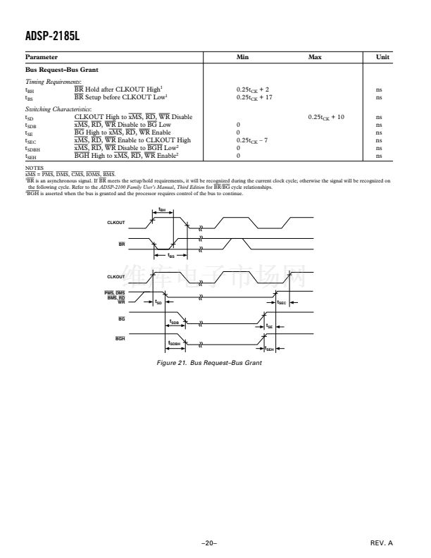
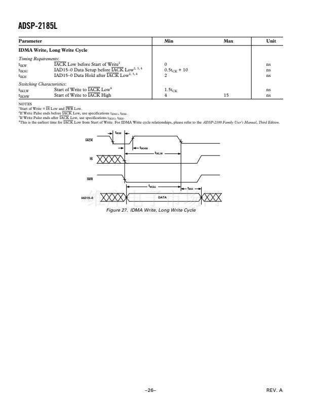
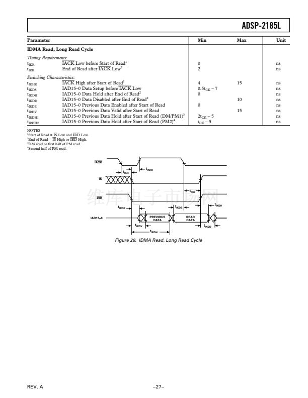
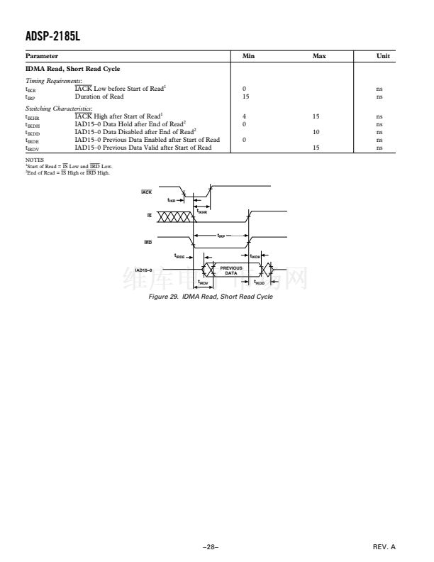
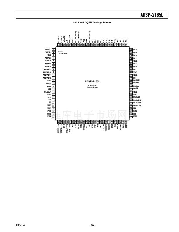
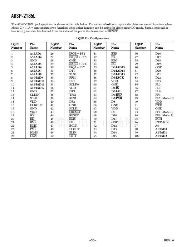
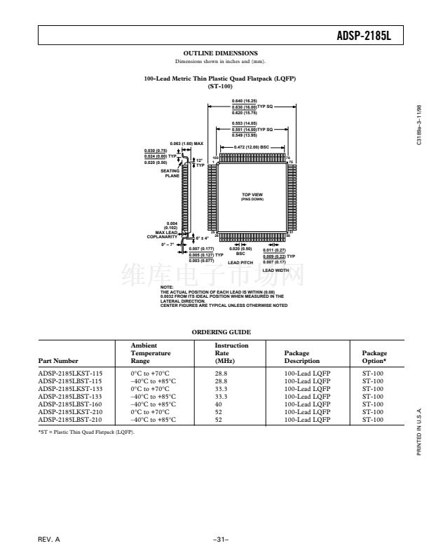
ADSP-2185L
Common-Mode Pin Descriptions
Memory Interface Pins
Pin
Name(s)
RESET
BR
BG
BGH
DMS
PMS
IOMS
BMS
CMS
RD
WR
IRQ2/
PF7
IRQL1/
PF6
IRQL0/
PF5
IRQE/
PF4
PF3
Mode C/
PF2
Mode B/
PF1
Mode A/
PF0
CLKIN,
XTAL
CLKOUT
SPORT0
SPORT1
IRQ1:0
FI, FO
PWD
PWDACK
FL0, FL1,
FL2
VDD and
GND
EZ-Port
N
OTES
1
# of Input/
Pins Output
1
1
1
1
1
1
1
1
1
1
1
1
1
1
1
I
I
O
O
O
O
O
O
O
O
O
I
I/O
I
I/O
I
I/O
I
I/O
I/O
I
I/O
1
I
I/O
1
I
I/O
Function
Processor Reset Input
Bus Request Input
Bus Grant Output
Bus Grant Hung Output
Data Memory Select Output
Program Memory Select Output
Memory Select Output
Byte Memory Select Output
Combined Memory Select Output
Memory Read Enable Output
Memory Write Enable Output
Edge- or Level-Sensitive Interrupt
Request.
1
Programmable I/O Pin
Level-Sensitive Interrupt Requests
1
Programmable I/O Pin
Level-Sensitive Interrupt Requests
1
Programmable I/O Pin
Edge-Sensitive Interrupt Requests
1
Programmable I/O Pin
Programmable I/O Pin During
Normal Operation
Mode Select Input鈥擟hecked
Only During
RESET
Programmable I/O Pin During
Normal Operation
Mode Select Input鈥擟hecked
Only During
RESET
Programmable I/O Pin During
Normal Operation
Mode Select Input鈥擟hecked
Only During
RESET
Programmable I/O Pin During
Normal Operation
Clock or Quartz Crystal Input
Processor Clock Output
Serial Port I/O Pins
Serial Port I/O Pins
Edge- or Level-Sensitive Interrupts,
Flag In, Flag Out
2
Power-Down Control Input
Power-Down Control Output
Output Flags
Power and Ground
For Emulation Use
The ADSP-2185L processor can be used in one of two modes,
Full Memory Mode, which allows BDMA operation with full
external overlay memory and I/O capability, or Host Mode,
which allows IDMA operation with limited external addressing
capabilities. The operating mode is determined by the state of
the Mode C pin during
RESET
and cannot be changed while
the processor is running. See tables for Full Memory Mode Pins
and Host Mode Pins for descriptions.
Full Memory Mode Pins (Mode C = 0)
Pin
# of Input/
Name(s) Pins Output Function
A13:0
D23:0
14
24
O
I/O
Address Output Pins for Program,
Data, Byte and I/O Spaces
Data I/O Pins for Program, Data,
Byte and I/O Spaces (8 MSBs are
also used as Byte Memory addresses)
Host Mode Pins (Mode C = 1)
Pin
# of Input/
Name(s) Pins Output Function
IAD15:0 16
A0
1
D23:8
IWR
IRD
IAL
IS
IACK
16
1
1
1
1
1
I/O
O
I/O
I
I
I
I
O
IDMA Port Address/Data Bus
Address Pin for External I/O, Pro-
gram, Data or Byte access
Data I/O Pins for Program, Data
Byte and I/O spaces
IDMA Write Enable
IDMA Read Enable
IDMA Address Latch Pin
IDMA Select
IDMA Port Acknowledge
1
In Host Mode, external peripheral addresses can be decoded using the A0,
CMS, PMS, DMS
and
IOMS
signals
Terminating Unused Pin
2
1
5
5
I
O
I/O
I/O
The following table shows the recommendations for terminating
unused pins.
Pin Terminations
Pin
Name
XTAL
CLKOUT
A13:1 or
IAD12:0
A0
D23:8
D7 or
IWR
D6 or
IRD
D5 or
IAL
I/O
3-State
(Z)
I
O
O (Z)
I/O (Z)
O (Z)
I/O (Z)
I/O (Z)
I
I/O (Z)
I
I/O (Z)
I
Reset
State
I
O
Hi-Z
Hi-Z
Hi-Z
Hi-Z
Hi-Z
I
Hi-Z
I
Hi-Z
I
Hi-Z*
Caused
By
Unused
Configuration
Float
Float
Float
Float
Float
Float
Float
High (Inactive)
Float
High (Inactive)
Float
Low (Inactive)
1
1
3
16
9
I
O
O
I
I/O
BR, EBR
IS
BR, EBR
BR, EBR
BR, EBR
BR, EBR
BR, EBR
Interrupt/Flag Pins retain both functions concurrently. If IMASK is set to enable the
corresponding interrupts, then the DSP will vector to the appropriate interrupt vec-
tor address when the pin is asserted, either by external devices, or set as a program-
mable flag.
2
SPORT configuration determined by the DSP System Control Register. Software
configurable.
prev
next


 1
1
 2
2
 3
3
 4
4
 5
5
 6
6
 7
7
 8
8
 9
9
 10
10
 11
11
 12
12
 13
13
 14
14
 15
15
 16
16
 17
17
 18
18
 19
19
 20
20
 21
21
 22
22
 23
23
 24
24
 25
25
 26
26
 27
27
 28
28
 29
29
 30
30
 31
31
