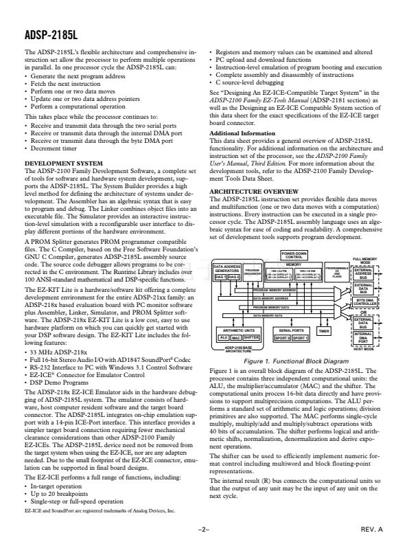
ADSP-2185L
LOW POWER OPERATION
The ADSP-2185L has three low power modes that significantly
reduce the power dissipation when the device operates under
standby conditions. These modes are:
鈥?Power-Down
鈥?Idle
鈥?Slow Idle
The CLKOUT pin may also be disabled to reduce external
power dissipation.
Power-Down
When the
IDLE (n)
instruction is used, it effectively slows down
the processor鈥檚 internal clock and thus its response time to in-
coming interrupts. The one-cycle response time of the standard
idle state is increased by
n,
the clock divisor. When an enabled
interrupt is received, the ADSP-2185L will remain in the idle
state for up to a maximum of
n
processor cycles (n = 16, 32, 64
or 128) before resuming normal operation.
When the
IDLE (n)
instruction is used in systems that have an
externally generated serial clock (SCLK), the serial clock rate
may be faster than the processor鈥檚 reduced internal clock rate.
Under these conditions, interrupts must not be generated at a
faster rate than can be serviced, due to the additional time the
processor takes to come out of the idle state (a maximum of
n
processor cycles).
SYSTEM INTERFACE
The ADSP-2185L processor has a low power feature that lets
the processor enter a very low power dormant state through
hardware or software control. Here is a brief list of power-down
features. Refer to the
ADSP-2100 Family User鈥檚 Manual, Third
Edition,
鈥淪ystem Interface鈥?chapter, for detailed information
about the power-down feature.
鈥?Quick recovery from power-down. The processor begins ex-
ecuting instructions in as few as 400 CLKIN cycles.
鈥?Support for an externally generated TTL or CMOS processor
clock. The external clock can continue running during power-
down without affecting the 400 CLKIN cycle recovery.
鈥?Support for crystal operation includes disabling the oscillator
to save power (the processor automatically waits 4096 CLKIN
cycles for the crystal oscillator to start and stabilize), and let-
ting the oscillator run to allow 400 CLKIN cycle start up.
鈥?Power-down is initiated by either the power-down pin (PWD)
or the software power-down force bit Interrupt support allows
an unlimited number of instructions to be executed before op-
tionally powering down. The power-down interrupt also can
be used as a non-maskable, edge-sensitive interrupt.
鈥?Context clear/save control allows the processor to continue
where it left off or start with a clean context when leaving the
power-down state.
鈥?The
RESET
pin also can be used to terminate power-down.
鈥?Power-down acknowledge pin indicates when the processor
has entered power-down.
Idle
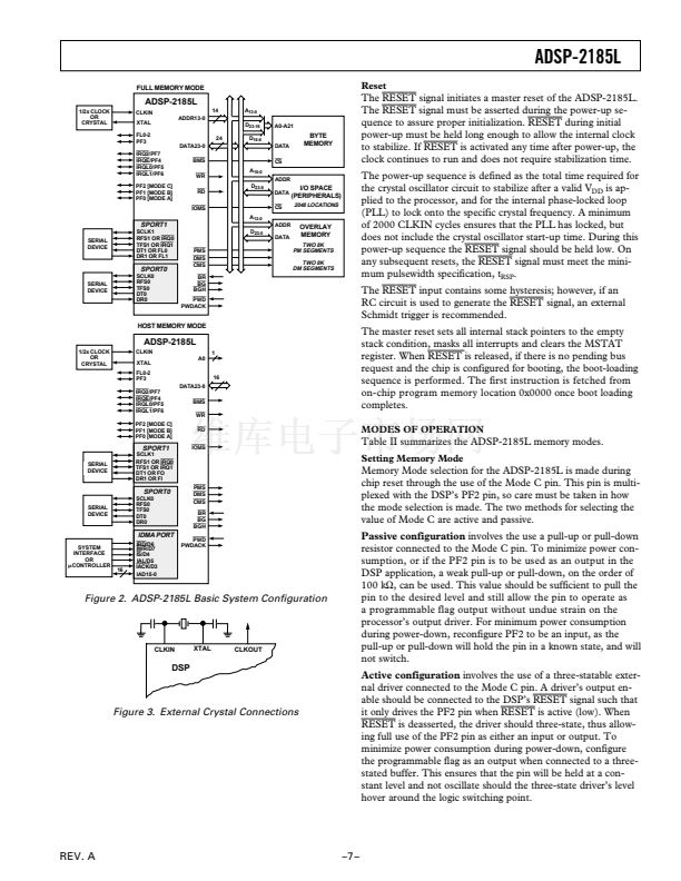
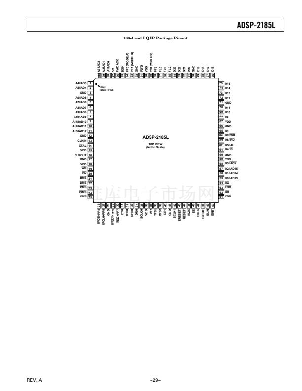
Figure 2 shows a typical basic system configuration with the
ADSP-2185L, two serial devices, a byte-wide EPROM, and
optional external program and data overlay memories (mode se-
lectable). Programmable wait state generation allows the proces-
sor to connect easily to slow peripheral devices. The ADSP-2185L
also provides four external interrupts and two serial ports or six
external interrupts and one serial port. Host Memory Mode al-
lows access to the full external data bus, but limits addressing to
a single address bit (A0). Additional system peripherals can be
added in this mode through the use of external hardware to gen-
erate and latch address signals.
Clock Signals
The ADSP-2185L can be clocked by either a crystal or a TTL-
compatible clock signal.
The CLKIN input cannot be halted, changed during operation
or operated below the specified frequency during normal opera-
tion. The only exception is while the processor is in the power-
down state. For additional information, refer to Chapter 9,
ADSP-2100 Family User鈥檚 Manual, Third Edition,
for detailed in-
formation on this power-down feature.
If an external clock is used, it should be a TTL-compatible sig-
nal running at half the instruction rate. The signal is connected
to the processor鈥檚 CLKIN input. When an external clock is
used, the XTAL input must be left unconnected.
The ADSP-2185L uses an input clock with a frequency equal to
half the instruction rate; a 26.00 MHz input clock yields a 19 ns
processor cycle (which is equivalent to 52 MHz). Normally, in-
structions are executed in a single processor cycle. All device
timing is relative to the internal instruction clock rate, which is
indicated by the CLKOUT signal when enabled.
Because the ADSP-2185L includes an on-chip oscillator circuit,
an external crystal may be used. The crystal should be connected
across the CLKIN and XTAL pins, with two capacitors connected
as shown in Figure 3. Capacitor values are dependent on crystal
type and should be specified by the crystal manufacturer. A
parallel-resonant, fundamental frequency, microprocessor-grade
crystal should be used.
A clock output (CLKOUT) signal is generated by the processor
at the processor鈥檚 cycle rate. This can be enabled and disabled
by the CLK0DIS bit in the SPORT0 Autobuffer Control Register.
When the ADSP-2185L is in the Idle Mode, the processor waits
indefinitely in a low power state until an interrupt occurs. When
an unmasked interrupt occurs, it is serviced; execution then con-
tinues with the instruction following the
IDLE
instruction. In
Idle Mode IDMA, BDMA and autobuffer cycle steals still occur.
Slow Idle
The
IDLE
instruction on the ADSP-2185L slows the processor鈥檚
internal clock signal, further reducing power consumption. The
reduced clock frequency, a programmable fraction of the nor-
mal clock rate, is specified by a selectable divisor given in the
IDLE
instruction. The format of the instruction is
IDLE (n);
where
n
= 16, 32, 64 or 128. This instruction keeps the proces-
sor fully functional, but operating at the slower clock rate. While
it is in this state, the processor鈥檚 other internal clock signals,
such as SCLK, CLKOUT and timer clock, are reduced by the
same ratio. The default form of the instruction, when no clock
divisor is given, is the standard
IDLE
instruction.
prev
next


 1
1
 2
2
 3
3
 4
4
 5
5
 6
6
 7
7
 8
8
 9
9
 10
10
 11
11
 12
12
 13
13
 14
14
 15
15
 16
16
 17
17
 18
18
 19
19
 20
20
 21
21
 22
22
 23
23
 24
24
 25
25
 26
26
 27
27
 28
28
 29
29
 30
30
 31
31
