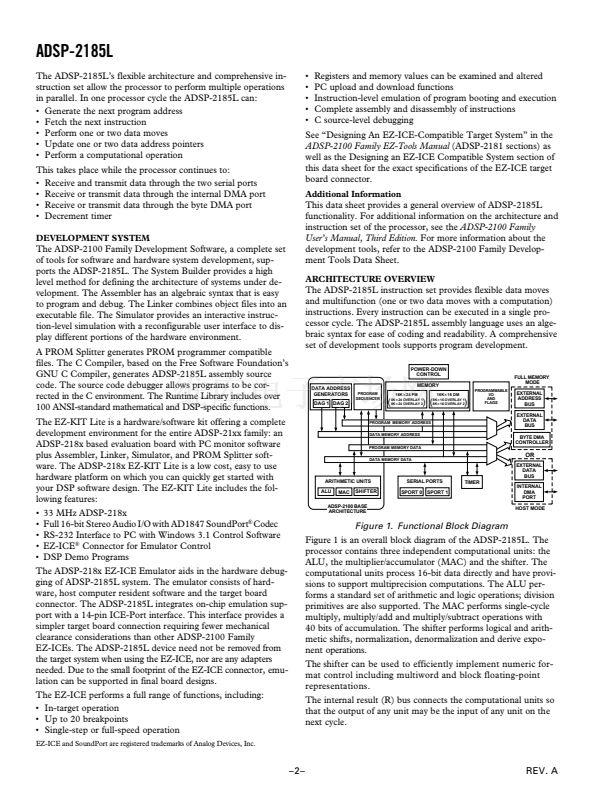
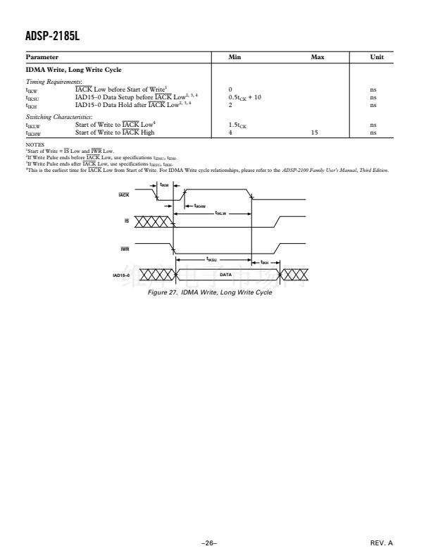
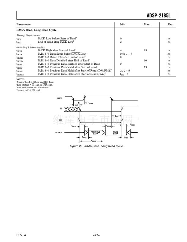
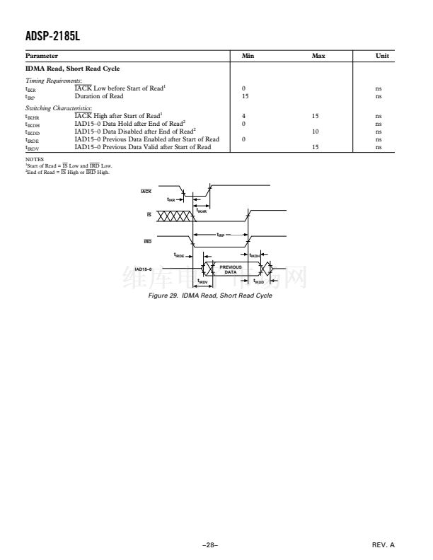
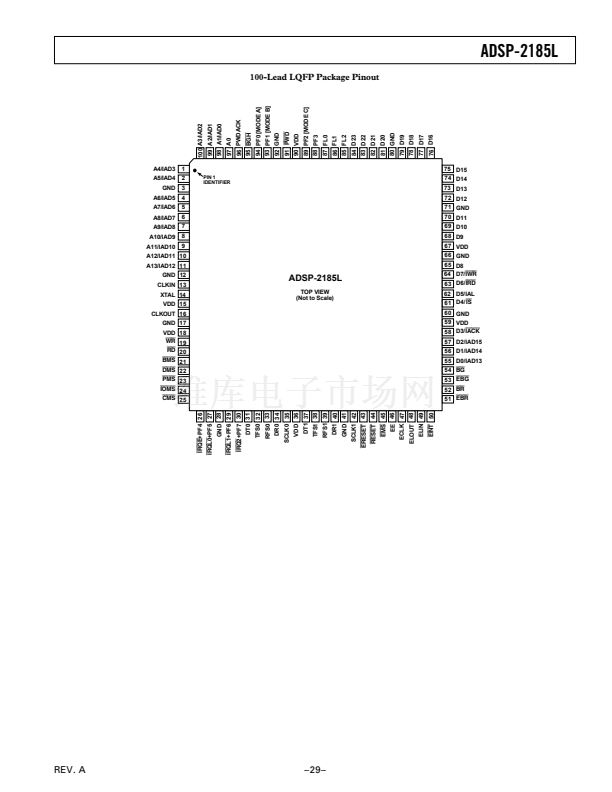
ADSP-2185L
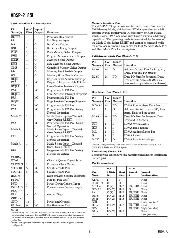
FULL MEMORY MODE
Reset
14
A
13-0
D
23-16
24
D
15-8
DATA
CS
A
10-0
ADDR
D
23-8
A0-A21
ADSP-2185L
1/2x CLOCK
OR
CRYSTAL
CLKIN
XTAL
FL0-2
PF3
IRQ2/PF7
IRQE/PF4
IRQL0/PF5
IRQL1/PF6
PF2 [MODE C]
PF1 [MODE B]
PF0 [MODE A]
ADDR13-0
DATA23-0
BMS
WR
RD
IOMS
A
13-0
BYTE
MEMORY
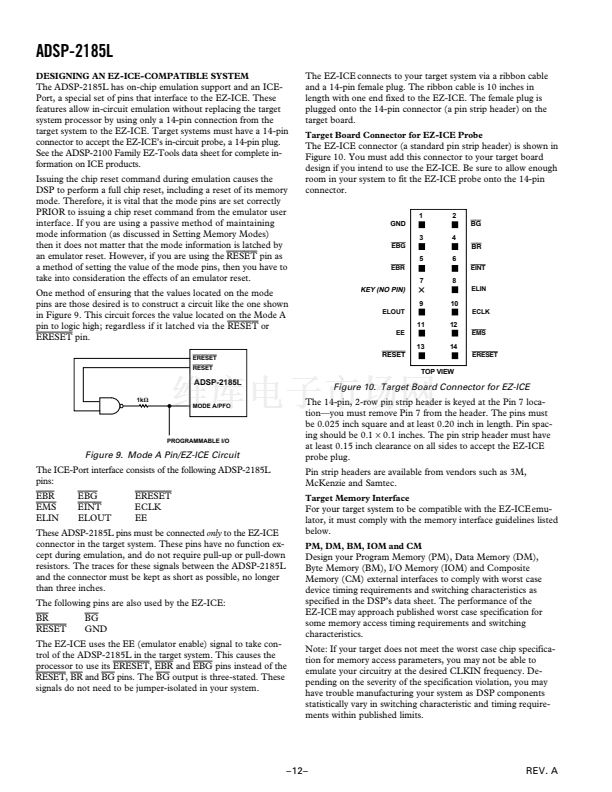
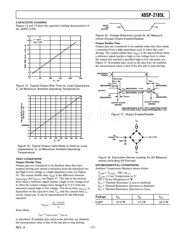
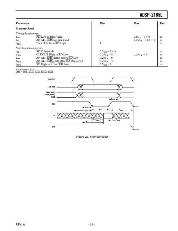
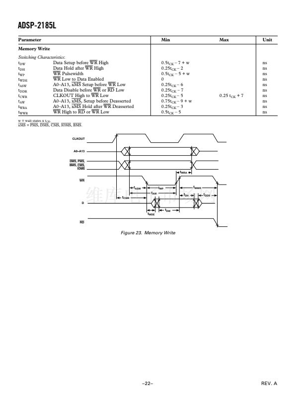
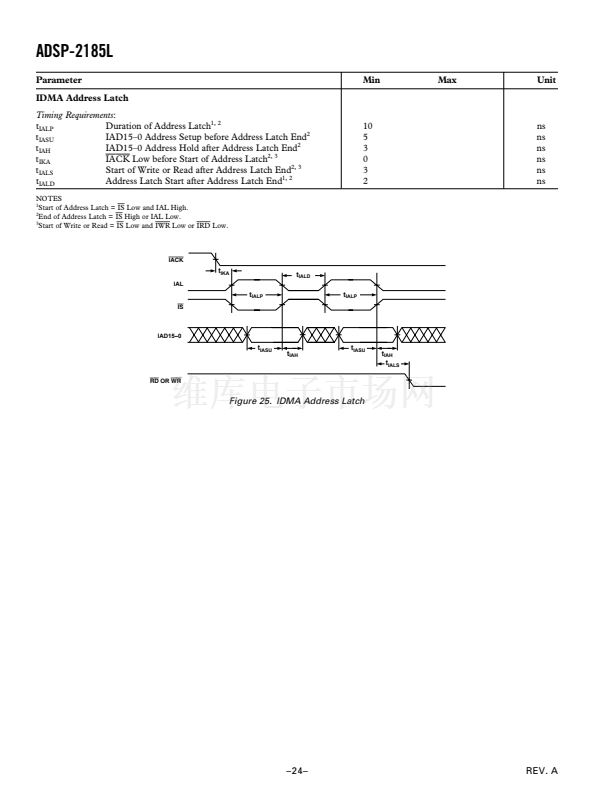
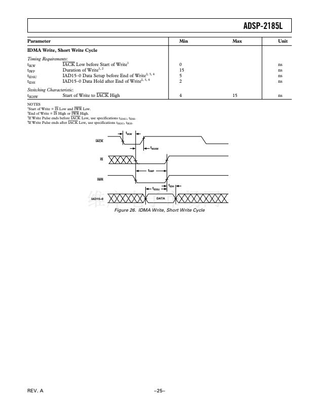
The
RESET
signal initiates a master reset of the ADSP-2185L.
The
RESET
signal must be asserted during the power-up se-
quence to assure proper initialization.
RESET
during initial
power-up must be held long enough to allow the internal clock
to stabilize. If
RESET
is activated any time after power-up, the
clock continues to run and does not require stabilization time.
The power-up sequence is defined as the total time required for
the crystal oscillator circuit to stabilize after a valid V
DD
is ap-
plied to the processor, and for the internal phase-locked loop
(PLL) to lock onto the specific crystal frequency. A minimum
of 2000 CLKIN cycles ensures that the PLL has locked, but
does not include the crystal oscillator start-up time. During this
power-up sequence the
RESET
signal should be held low. On
any subsequent resets, the
RESET
signal must meet the mini-
mum pulsewidth specification, t
RSP
.
The
RESET
input contains some hysteresis; however, if an
RC circuit is used to generate the
RESET
signal, an external
Schmidt trigger is recommended.
The master reset sets all internal stack pointers to the empty
stack condition, masks all interrupts and clears the MSTAT
register. When
RESET
is released, if there is no pending bus
request and the chip is configured for booting, the boot-loading
sequence is performed. The first instruction is fetched from
on-chip program memory location 0x0000 once boot loading
completes.
MODES OF OPERATION
I/O SPACE
DATA
(PERIPHERALS)
CS
ADDR
2048 LOCATIONS
SPORT1
SERIAL
DEVICE
SCLK1
RFS1 OR
IRQ0
TFS1 OR
IRQ1
DT1 OR FL0
DR1 OR FL1
D
23-0
DATA
PMS
DMS
CMS
BR
BG
BGH
PWD
PWDACK
OVERLAY
MEMORY
TWO 8K
PM SEGMENTS
TWO 8K
DM SEGMENTS
SPORT0
SERIAL
DEVICE
SCLK0
RFS0
TFS0
DT0
DR0
HOST MEMORY MODE
ADSP-2185L
1/2x CLOCK
OR
CRYSTAL
CLKIN
XTAL
FL0-2
PF3
IRQ2/PF7
IRQE/PF4
IRQL0/PF5
IRQL1/PF6
PF2 [MODE C]
PF1 [MODE B]
PF0 [MODE A]
DATA23-8
BMS
WR
RD
IOMS
A0
1
16
SPORT1
SERIAL
DEVICE
SCLK1
RFS1 OR
IRQ0
TFS1 OR
IRQ1
DT1 OR FO
DR1 OR FI
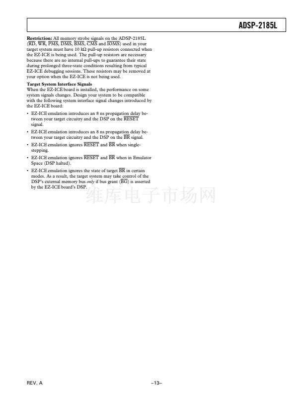
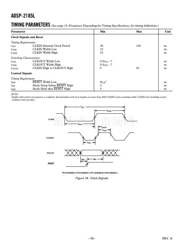
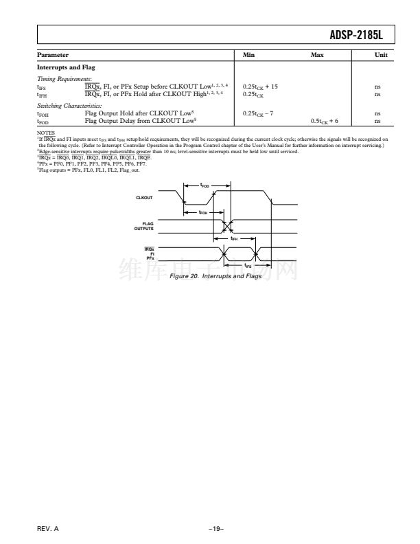
Table II summarizes the ADSP-2185L memory modes.
Setting Memory Mode
SPORT0
SERIAL
DEVICE
SCLK0
RFS0
TFS0
DT0
DR0
PMS
DMS
CMS
BR
BG
BGH
PWD
PWDACK
Memory Mode selection for the ADSP-2185L is made during
chip reset through the use of the Mode C pin. This pin is multi-
plexed with the DSP鈥檚 PF2 pin, so care must be taken in how
the mode selection is made. The two methods for selecting the
value of Mode C are active and passive.
Passive configuration
involves the use a pull-up or pull-down
resistor connected to the Mode C pin. To minimize power con-
sumption, or if the PF2 pin is to be used as an output in the
DSP application, a weak pull-up or pull-down, on the order of
100 k鈩? can be used. This value should be sufficient to pull the
pin to the desired level and still allow the pin to operate as
a programmable flag output without undue strain on the
processor鈥檚 output driver. For minimum power consumption
during power-down, reconfigure PF2 to be an input, as the
pull-up or pull-down will hold the pin in a known state, and will
not switch.
Active configuration
involves the use of a three-statable exter-
nal driver connected to the Mode C pin. A driver鈥檚 output en-
able should be connected to the DSP鈥檚
RESET
signal such that
it only drives the PF2 pin when
RESET
is active (low). When
RESET
is deasserted, the driver should three-state, thus allow-
ing full use of the PF2 pin as either an input or output. To
minimize power consumption during power-down, configure
the programmable flag as an output when connected to a three-
stated buffer. This ensures that the pin will be held at a con-
stant level and not oscillate should the three-state driver鈥檚 level
hover around the logic switching point.
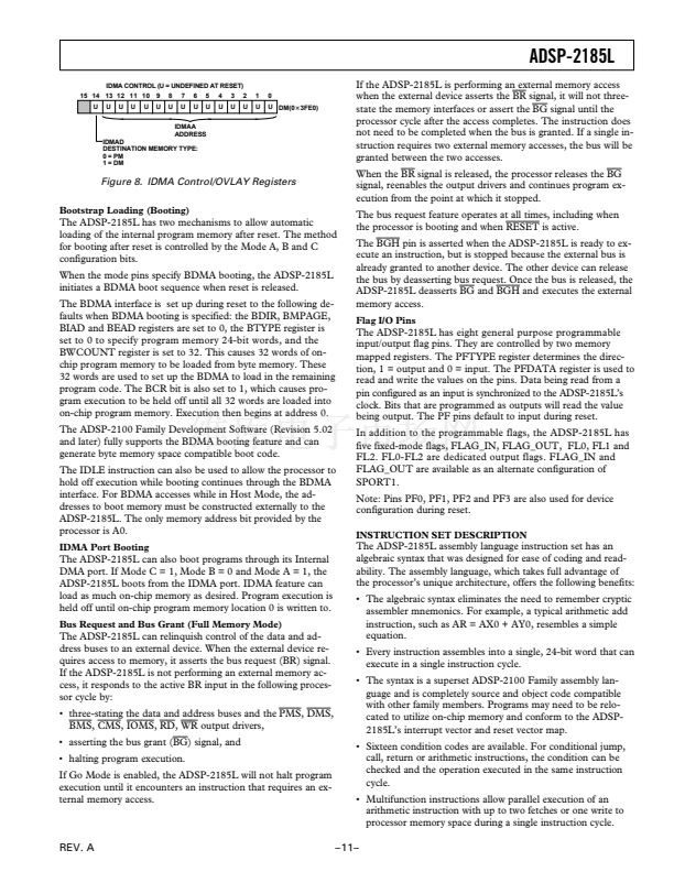
IDMA PORT
SYSTEM
INTERFACE
OR
CONTROLLER
IRD/D6
IWR/D7
IS/D4
IAL/D5
IACK/D3
IAD15-0
16
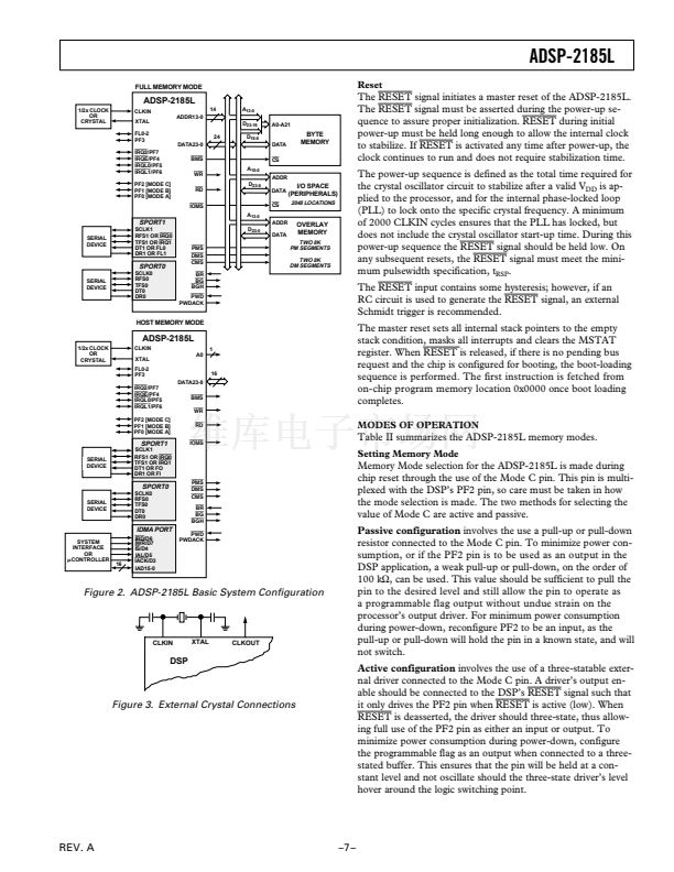
Figure 2. ADSP-2185L Basic System Configuration
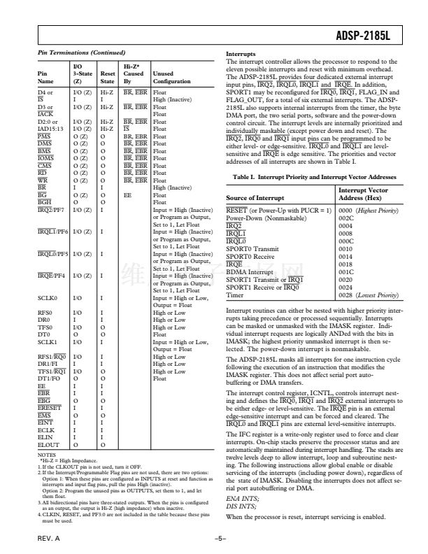
CLKIN
XTAL
CLKOUT
DSP
Figure 3. External Crystal Connections
REV. A
鈥?鈥?/div>
prev
next


 1
1
 2
2
 3
3
 4
4
 5
5
 6
6
 7
7
 8
8
 9
9
 10
10
 11
11
 12
12
 13
13
 14
14
 15
15
 16
16
 17
17
 18
18
 19
19
 20
20
 21
21
 22
22
 23
23
 24
24
 25
25
 26
26
 27
27
 28
28
 29
29
 30
30
 31
31
