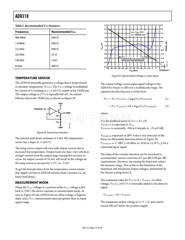
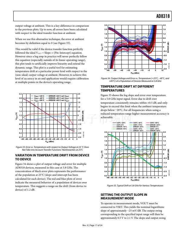
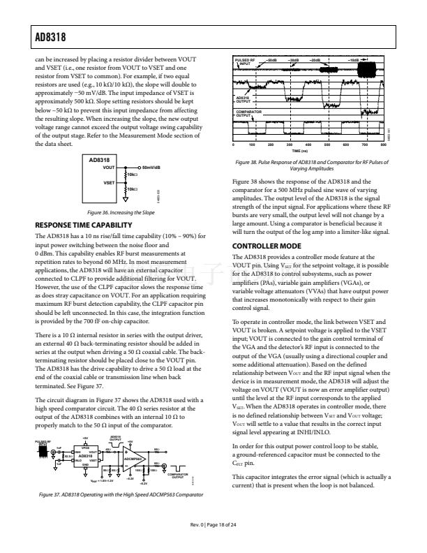
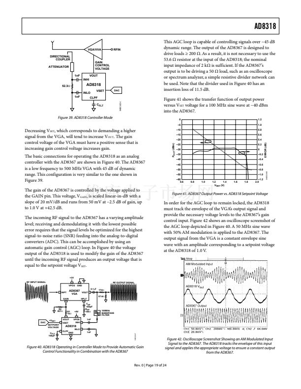
Figure 25. Output Interface
鈩?/div>
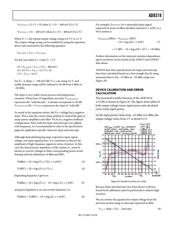
for optimal temperature
compensation at 2.2 GHz input frequency, is connected
between this pin and ground (see Figure 22). The value of
this resistor partially determines the magnitude of an analog
correction coefficient, which is employed to reduce
intercept drift.
Table 5 lists recommended resistors for other frequencies.
These resistors have been chosen to provide the best overall
temperature drift based on measurements of a diverse
population of devices.
The relationship between output temperature drift and
frequency is not linear and cannot be easily modeled. As a
result, experimentation is required to choose the correct
T
ADJ
resistor at frequencies not listed in Table 5.
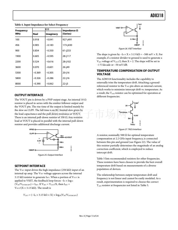
SETPOINT INTERFACE
The V
SET
input drives the high impedance (250 k鈩? input of an
internal op amp. The V
SET
voltage appears across the internal
3.13 k鈩?resistor to generate I
SET
. When a portion of V
OUT
is
applied to VSET, the feedback loop forces 鈭扞
D
脳 log
10
(V
IN
/V
INTERCEPT
) = I
SET
. If V
SET
= V
OUT
/X, then I
SET
=
V
OUT
/(X 脳 3.13 k鈩?. The result is
V
OUT
= (鈭扞
D
脳 3.13 k鈩?脳 X) 脳 log
10
(V
IN
/V
INTERCEPT
)
Rev. 0 | Page 13 of 24


 1
1
 2
2
 3
3
 4
4
 5
5
 6
6
 7
7
 8
8
 9
9
 10
10
 11
11
 12
12
 13
13
 14
14
 15
15
 16
16
 17
17
 18
18
 19
19
 20
20
 21
21
 22
22
 23
23
 24
24
