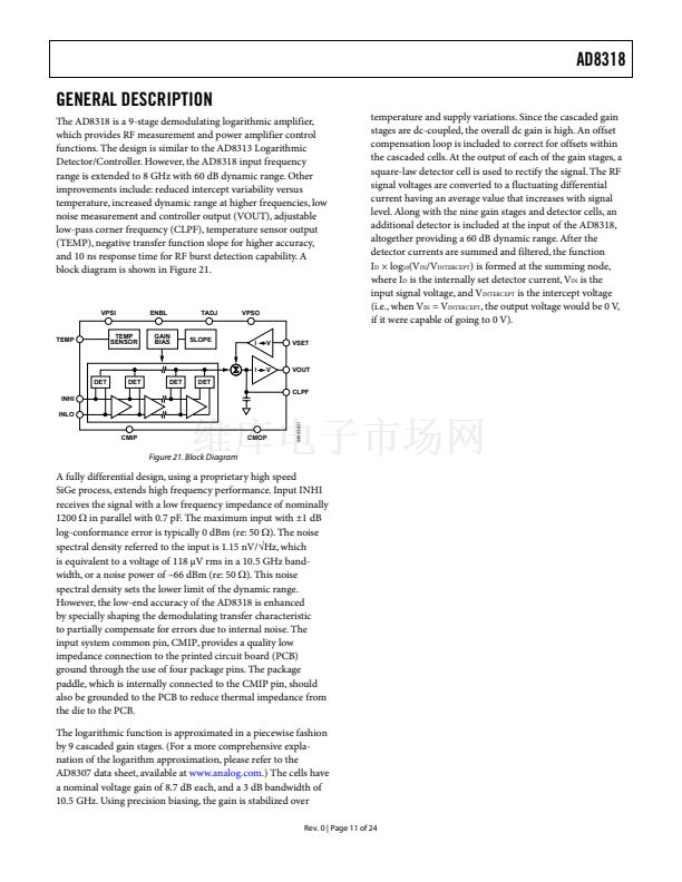
When X = 1, the typical output voltage swing is 0.5 V to 2.1 V.
鈥?6 dBm.
variation. When base-10 logarithms are used, V
represents the slope in 鈥渧olts/dB.鈥?/div>
As noted in the equations above, the V
OUT
voltage has a negative
slope. This is also the correct slope polarity to control the gain of
many power amplifiers and other VGAs in a negative feedback
configuration. Since both the slope and intercept vary slightly
with frequency, it is recommended to refer to the specification
pages for application specific values for slope and intercept.
Although demodulating log amps respond to input signal
voltage, not input signal power, it is customary to discuss the
amplitude of high frequency signals in terms of power. In this
case, the characteristic impedance of the system, Z
o
, must be
known to convert voltages to their corresponding power levels.
Starting with the definitions of dBm and dBV,
P(dBm) = 10 脳 log
10
(V
rms2
/(Z
O
脳 1 mW))
V(dBV) = 20 脳 log
10
(V
rms
/1 V
rms
)
Expanding Equation 3 gives us:
P(dBm) = 20 脳 log
10
(V
rms
) 鈭?10 脳 log
10
( Z
O
脳 1 mW)
and given Equation 4, we can rewrite Equation 5 as
P(dBm) = V(dBV) 鈭?10 脳 log
10
(Z
O
脳 1 mW)
(6)
We can rewrite the equation for output voltage from the
previous section using an intercept expressed in dBm
V
OUT
=
Slope
脳 (P
IN
鈥?/div>
Intercept)
Rev. 0 | Page 15 of 24
For example, P
INTERCEPT
for a sinusoidal input signal
expressed in terms of dBm (decibels referred to 1 mW), in a
50 鈩?system is:
P
INTERCEPT
(dBm) = V
INTERCEPT
(dBV)
鈥?10 脳 log
10
(Zo 脳 1 mW)
(7)
= +7 dBV 鈭?10 脳 log
10
(50 脳 10
-3
) = +20 dBm
Further information on the intercept variation dependence
upon waveform can be found in the AD8313 and AD8307
data sheets.
AD8318 data sheet specifications for slope and intercept
have been calculated based on a best straight line fit using
measured data in the 鈭?0 dBm to 鈭?0 dBm range (see
Figure 29).
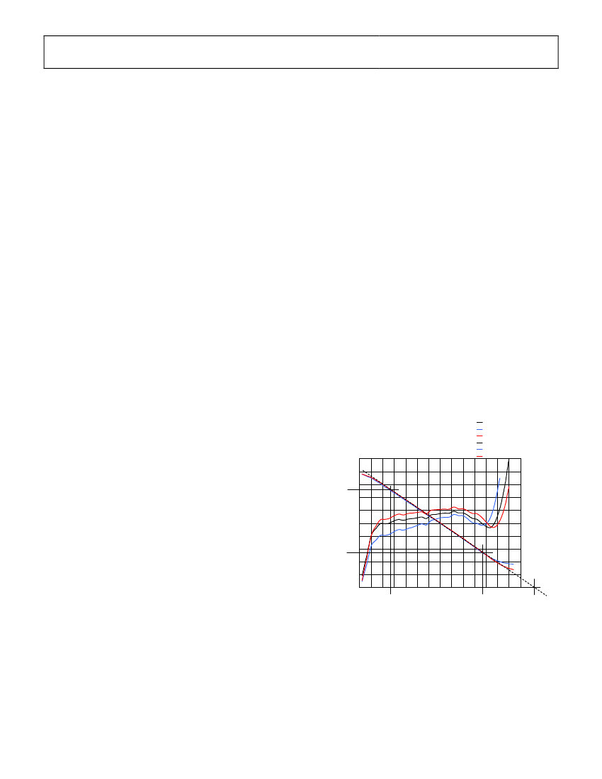
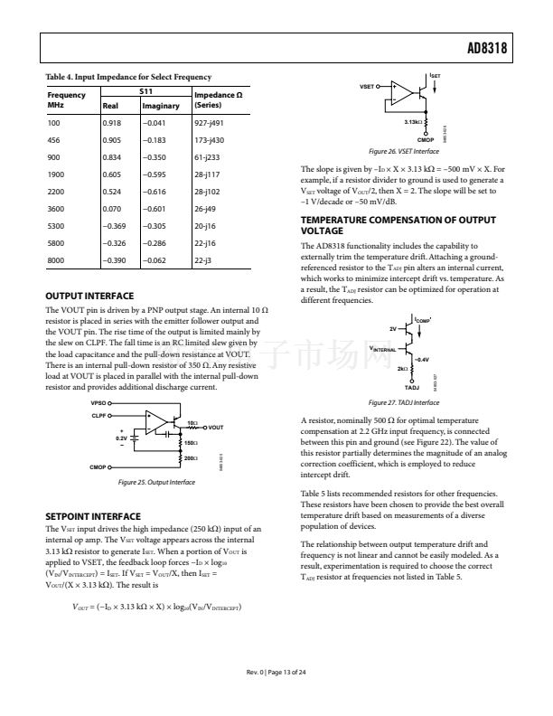
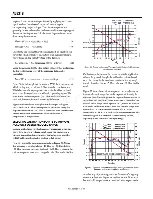
DEVICE CALIBRATION AND ERROR
CALCULATION
The measured transfer function of the AD8318 at
2.2 GHz is shown in
Figure 30
. The figure shows plots of
both output voltage versus input power and calculated
error versus input power.
As the input power varies from
鈭?/div>
65 dBm to 0 dBm, the
output voltage varies from 2 V to about 0.5 V.
VOUT
IDEAL
= SLOPE
脳
(P
IN
鈥?INTERCEPT)
SLOPE = (VOUT
1
鈥?VOUT
2
)/(PIN
1
鈥?PIN
2
)
INTERCEPT = PIN
1
鈥?(VOUT
1
/SLOPE)
ERROR (dB) = (VOUT
脳
VOUT
IDEAL
)/SLOPE
V
OUT
+25掳C
V
OUT
鈥?0掳C
V
OUT
+85掳C
ERROR +25掳C
ERROR 鈥?0掳C
ERROR +85掳C
2.2
2.0
1.8
VOUT
2
1.6
1.4
V
OUT
(V)
2.5
2.0
1.5
1.0
ERROR (dB)
0.5
0
鈥?.5
鈥?.0
鈥?.5
鈥?.0
鈥?
0
1.2
1.0
0.8
0.6
(3)
(4)
VOUT
1
0.4
0.2
鈥?5 鈥?0 鈥?5
鈥?5 鈥?0 鈥?5 鈥?0 鈥?5 鈥?0 鈥?5
PIN
1
PIN
2
P
IN
(dBm)
5
INTERCEPT
(5)
Figure 30. Transfer Function at 2.2 GHz
Because slope and intercept vary from device to device,
board-level calibration must be performed to achieve high
accuracy.
(8)
04853-030


 1
1
 2
2
 3
3
 4
4
 5
5
 6
6
 7
7
 8
8
 9
9
 10
10
 11
11
 12
12
 13
13
 14
14
 15
15
 16
16
 17
17
 18
18
 19
19
 20
20
 21
21
 22
22
 23
23
 24
24
