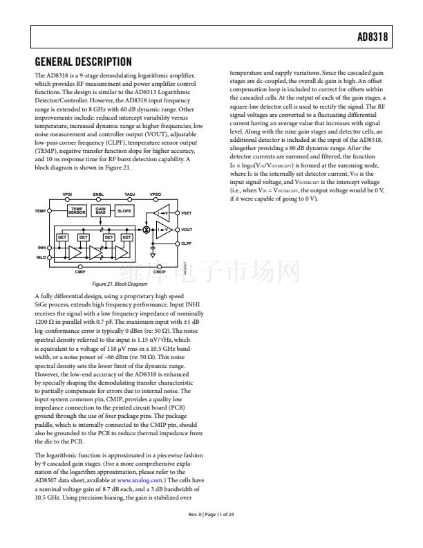
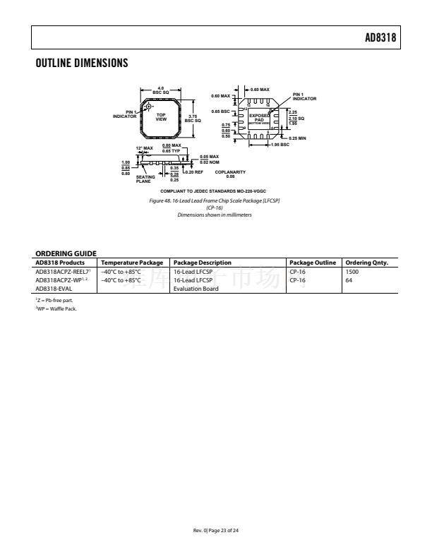
AD8318
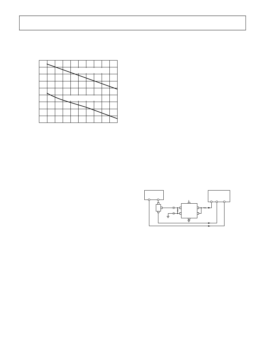
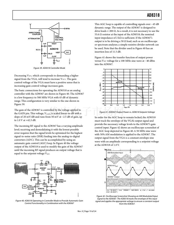
The 45 dB control range is constant for the range of V
SET
voltages. The input power levels to the AD8367 must be
optimized to achieve this range. In Figure 43 the minimum and
maximum input power levels are shown vs. setpoint voltage.
10
0
MAXIMUM INPUT LEVEL
鈥?0
鈥?0
CHARACTERIZATION SETUPS AND METHODS
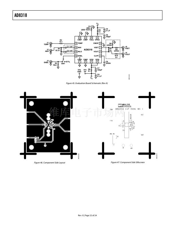
The general hardware configuration used for the AD8318
characterization is shown in Figure 45. The primary setup
used for characterization was measurement mode. The
characterization board is similar to the customer evaluation
board with the exception that the RFIN had a Rosenberger
SMA connector and R10 was changed to a 1 k鈩?resistor to
remove cable capacitance from the bench characterization
setup. Slope and intercept were calculated using linear
regression from 鈭?0 dBm to 鈭?0 dBm. The slope and
intercept are used to generate an ideal line. Log conform-
ance error is the difference from the ideal line and the
measured output voltage for a given temperature in dB. For
additional information on the error calculation, refer to the
Device Calibration and Error Calculation section.
The hardware configuration for pulse response measure-
ment replaced the 0 鈩?series resistor on the VOUT pin with
a 40 鈩?resistor and the CLPF pin was left open. Pulse
response time was measured using a Tektronix TDS51504
Digital Phosphor Oscilloscope. Both channels on the scope
had 50 鈩?termination selected. The 10 鈩?internal to the
output interface and the 40 鈩?series resistor attenuate the
output response by 2. RF input frequency was 100 MHz
with 鈭?0 dBm at the input of the device. The RF burst was
generated using SMT06 with the pulse option with a period
of 1.5 碌S, a width of 0.1 碌S, and a pulse delay of 0.04 碌S. The
output response was triggered using the video out from the
SMT06. Refer to Figure 44 for an overview of the test setup.
R AND S SMT06
VIDEO
OUT
RF OUT
鈥?dBm
3dB
SPLITTER 1nF
INHI
52.3鈩?/div>
1nF
5V
P
IN
(dBm)
鈥?0
鈥?0
MINIMUM INPUT LEVEL
鈥?0
鈥?0
鈥?0
鈥?0
0.5
04853-049
0.6
0.7
0.8
0.9
1.0
1.2
V
SET
(V)
1.2
1.3
1.4
1.5
Figure 43. Setpoint Voltage vs. Input Power. Optimal signal levels must be
used to achieve the full 45 dB dynamic range capabilities of the AD8367.
In some cases, it may be found that if V
GAIN
is >1.0 V it may take
an unusually long time for the AGC loop to recover; that is, the
output of the AD8318 will remain at an abnormally high value
and the gain will be set to its maximum level. A voltage divider is
placed between the output of the AD8318 and the AD8367鈥檚
GAIN pin to ensure that V
GAIN
will not exceed 1.0 V.
In Figure 40, C
HP
and R
HP
are configured to reduce oscillation
and distortion due to harmonics at higher gain settings. Some
additional filtering is recommended between the output of the
AD8367 and the input of the AD8318. This will help to decrease
the output noise of the AD8367, which may reduce the dynamic
range of the loop at higher gain settings (smaller V
SET
).
Response time and the amount of signal integration are
controlled by C
FLT
鈥攖his functionality is analogous to the
feedback capacitor around an integrating amplifier. While it is
possible to use large capacitors for C
FLT
, in most applications
values under 1 nF will provide sufficient filtering.
Calibration in controller mode is similar to the method used in
measurement mode. A simple two-point calibration can be done
by applying two known V
SET
voltages or DAC codes and
measuring the output power from the VGA. Slope and intercept
can then be calculated with the following equations.
Slope
= (V
SET1
鈭?/div>
V
SET2
)/(P
OUT1
鈭?/div>
P
OUT2
)
Intercept
=
P
OUT1
鈭?/div>
V
SET1
/Slope
V
SET
=
Slope
脳 (Px 鈭?/div>
Intercept)
More information on AGC applications can be found in the
AD8367 Data Sheet.
(13)
(14)
(15)
TEKTRONIX
TDS51504
CH1* CH3* TRIGGER
*50鈩?/div>
TERMINATION
VPOS
VOUT
VSET
GND
40鈩?/div>
AD8318
INLO
Figure 44. Pulse Response Measurement Test Setup
To measure noise spectral density, the evaluation replaced
the 0 鈩?resistor in series with the VOUT pin with a 1 碌F dc
blocking capacitor. The capacitor was used because the
FSEA cannot handle dc voltages at the RF input. The CLPF
pin was left open for data collected for Figure 18. For
Figure 19 a 1 碌F capacitor was placed between CLPF and
ground. The large capacitor filtered the noise from the
detector stages of the log amp. Noise spectral density
measurements were made using R&S spectrum analyzer
FSEA and R&S SMT06 signal generator. The signal
generator鈥檚 frequency was set to 2.2 GHz. The spectrum
analyzer had a span of 10 Hz, resolution bandwidth of
50 Hz, video bandwidth of 50 Hz, and averaged the signal
100 times. Data was adjusted to account for the dc blocking
capacitor impedance on the output at lower frequencies.
Rev. 0 | Page 20 of 24
04853-046
AD8318相关型号PDF文件下载
-
型号
版本
描述
厂商
下载
-
英文版
High Speed, Video Difference Amplifier
AD
-
英文版
High Speed, Video Difference Amplifier
AD [ Analog De...
-
英文版
High Supply, Video Difference Amplifier
-
英文版
Low Distortion Mixer
AD
-
英文版
Low Distortion Mixer
-
英文版
500 MHz Four-Quadrant Multiplier
AD
-
英文版
500 MHz Four-Quadrant Multiplier
-
英文版
250 MHz, Voltage Output 4-Quadrant Multiplier
AD
-
英文版
250 MHz Voltage Output 4-Quadrand Multiplier
-
英文版
+3 Volt, Serial Input Complete 12-Bit DAC
AD
-
英文版
+3 Volt, Serial Input Complete 12-Bit DAC
AD [ Analog De...
-
英文版
+3 Volt, Serial Input Complete 12-Bit DAC
-
英文版
-
英文版
LF.2.7 GHz RF/IF Gain and Phase Detector
AD [ Analog De...
-
英文版
LF.2.7 GHz RF/IF Gain and Phase Detector
AD
-
英文版
+3 V, Dual, Serial Input Complete 12-Bit DAC
AD
-
英文版
+ 3V, Dual, Serial Input Complete 12-Bit DAC
-
英文版
-
英文版
160 dB Range (100 pA -10 mA) Logarithmic Converter
AD
-
英文版
100 dB Range (10 nA to 1 mA) Logarithmic Converter
AD


 1
1
 2
2
 3
3
 4
4
 5
5
 6
6
 7
7
 8
8
 9
9
 10
10
 11
11
 12
12
 13
13
 14
14
 15
15
 16
16
 17
17
 18
18
 19
19
 20
20
 21
21
 22
22
 23
23
 24
24
