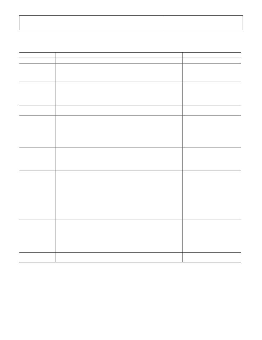
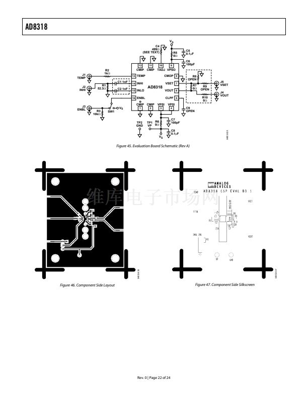
Table 6. Evaluation Board (Rev A) Configuration Options
AD8318 is in operating mode. In position B, the ENBL pin is grounded
through R3, putting the device in power-down mode. The ENBL pin may be
exercised by a pulse generator connected to J3 with SW1 in position B.
鈩?/div>
resistor in position R1 combines with the
AD8318's internal input impedance to give a broadband input impedance
of around 50
鈩?
Capacitors C1 and C2 are DC blocking capacitors. A reactive
impedance match can be implemented by replacing R1 with an inductor
and C1 and C2 with appropriately-valued capacitors .
Temperature Sensor Interface: The temperature sensor output voltage is
available at J1, via the current limiting resistor, R2.
Temperature Compensation Interface: The internal temperature
compensation resistor is optimized for an input signal of 2.2 GHz when C4 is
1 k鈩? This circuit can be adjusted to optimize performance for other input
frequencies by changing the value of the resistor in position C4. Note that
the designation C4 on the evaluation board is a typographical error as this
pad will always be populated with a resistor. This error will be corrected on
the Rev B revision of the board.
Output Interface鈥擬easurement Mode: In measurement mode, a portion of
the output voltage is fed back to pin VSET via R7. The magnitude of the
slope of the VOUT output voltage response may be increased by reducing
the portion of VOUT that is fed back to VSET. R10 can be used as a back-
terminating resistor or as part of a single-pole low-pass filter.
Output Interface鈥擟ontroller Mode: In this mode, R7 must be open. In
controller mode, the AD8318 can control the gain of an external
component. A setpoint voltage is applied to pin VSET, the value of which
corresponds to the desired RF input signal level applied to the AD8318 RF
input. A sample of the RF output signal from this variable-gain component is
selected, typically via a directional coupler, and applied to AD8318 RF input.
The voltage at pin VOUT is applied to the gain control of the variable gain
element. A control voltage is applied to pin VSET via R9 and R8. The
magnitude of the control voltage may optionally be attenuated via the
voltage divider comprised of R8 and R9, or a capacitor may be installed in
position R8 to form a low-pass filter along with R9.
Power Supply Decoupling: The nominal supply decoupling consists of a
100 pF filter capacitor placed physically close to the AD8318, a 0
鈩?/div>
series
resistor and a 0.1 碌F capacitor placed nearer to the power supply input pin.
Default Conditions
Not Applicable
SW1 = A
R3 = 10k (Size 0603)
R1 = 52.3
鈩?/div>
(Size 0402)
C1 = 1 nF (Size 0402)
C2 = 1 nF (Size 0402)
R1, C1, C2
R2
C4
C4 = 500 k鈩?(Size 0603)
R7, R8, R9, R10
R7 = 0
鈩?/div>
= (Size 0402)
R8 = open (Size 0402)
R9 = open (Size 0402
R10= 0
鈩?/div>
(Size 0402)
R7 = open (Size 0402)
R8 = open (Size 0402)
R9 = 0
鈩?/div>
(Size 0402)
R10 = 0
鈩?/div>
(Size 0402)
R7, R8, R9, R10
C5, C6, C7, C8, R5,
R6
C9
Filter Capacitor: The low-pass corner frequency of the circuit that drives pin
VOUT can be lowered by placing a capacitor between CLPF and ground.
C6 = 100 pF (Size 0402)
C7 = 100 pF (Size 0402)
C5 = 0.1 碌F (Size 0603)
C8 = 0.1 碌F (Size 0603)
R5 = 0
鈩?/div>
(Size 0603)
R6 = 0
鈩?/div>
(Size 0603)
C4 = open (Size 0603)
Rev. 0| Page 21 of 24
AD8318相关型号PDF文件下载
-
型号
版本
描述
厂商
下载
-
英文版
High Speed, Video Difference Amplifier
AD
-
英文版
High Speed, Video Difference Amplifier
AD [ Analog De...
-
英文版
High Supply, Video Difference Amplifier
-
英文版
Low Distortion Mixer
AD
-
英文版
Low Distortion Mixer
-
英文版
500 MHz Four-Quadrant Multiplier
AD
-
英文版
500 MHz Four-Quadrant Multiplier
-
英文版
250 MHz, Voltage Output 4-Quadrant Multiplier
AD
-
英文版
250 MHz Voltage Output 4-Quadrand Multiplier
-
英文版
+3 Volt, Serial Input Complete 12-Bit DAC
AD
-
英文版
+3 Volt, Serial Input Complete 12-Bit DAC
AD [ Analog De...
-
英文版
+3 Volt, Serial Input Complete 12-Bit DAC
-
英文版
-
英文版
LF.2.7 GHz RF/IF Gain and Phase Detector
AD [ Analog De...
-
英文版
LF.2.7 GHz RF/IF Gain and Phase Detector
AD
-
英文版
+3 V, Dual, Serial Input Complete 12-Bit DAC
AD
-
英文版
+ 3V, Dual, Serial Input Complete 12-Bit DAC
-
英文版
-
英文版
160 dB Range (100 pA -10 mA) Logarithmic Converter
AD
-
英文版
100 dB Range (10 nA to 1 mA) Logarithmic Converter
AD


 1
1
 2
2
 3
3
 4
4
 5
5
 6
6
 7
7
 8
8
 9
9
 10
10
 11
11
 12
12
 13
13
 14
14
 15
15
 16
16
 17
17
 18
18
 19
19
 20
20
 21
21
 22
22
 23
23
 24
24
