AD8318
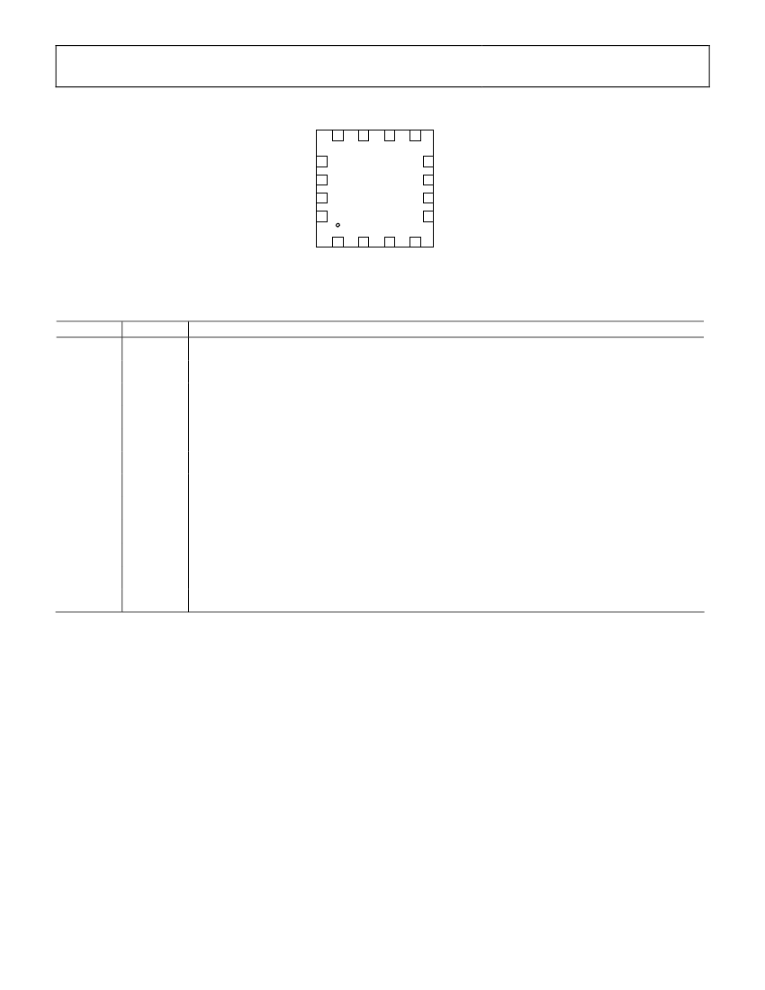
PIN CONFIGURATION AND FUNCTIONAL DESCRIPTIONS
12
11
10
9
CMIP CMIP TADJ VPSO
13
14
15
16
TEMP
INHI
CMOP
8
VSET
7
AD8318
INLO
ENBL
CMIP CMIP
1
2
VOUT
6
CLPF
5
VPSI
3
VPSI
4
Figure 2. 16-Lead Lead Frame Chip Scale Package (LFCSP)
Table 3. Pin Function Descriptions
Pin No.
1, 2, 11, 12
3, 4, 9
5
6
7
8
10
13
14
15
16
Mnemonic
CMIP
VPSI, VPSO
CLPF
VOUT
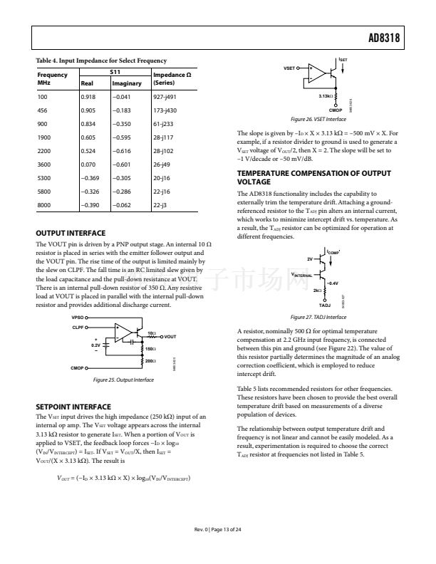
VSET
CMOP
TADJ
TEMP
INHI
INLO
ENBL
Paddle
Function
Device Common (Input System Ground).
Positive Supply Voltage for the Device Input System: 4.5 V to 5.5 V (voltage on all pins should be equal).
Loop Filter Capacitor.
Measurement and Controller Output.
Setpoint Input for Controller Mode, or Feedback Input for Measurement Mode.
Device Common (Output System Ground).
Temperature Compensation Adjustment.
Temperature Sensor Output.
RF Input. Nominal input range: 鈭?0 dBm to 0 dBm re: 50
鈩?
ac-coupled RF input.
RF Common for INHI; ac-coupled RF common.
Device Enable. Connect to VPSI for normal operation. Connect pin to ground for disable mode.
Internally Connected to CMIP, Solder to Ground.
Rev. 0 | Page 7 of 24
04853-002


 1
1
 2
2
 3
3
 4
4
 5
5
 6
6
 7
7
 8
8
 9
9
 10
10
 11
11
 12
12
 13
13
 14
14
 15
15
 16
16
 17
17
 18
18
 19
19
 20
20
 21
21
 22
22
 23
23
 24
24
