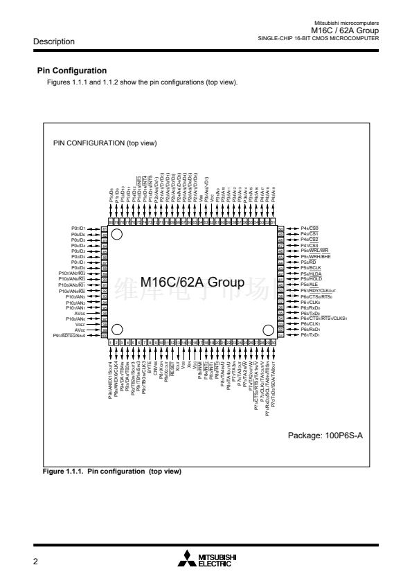
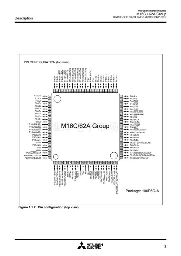
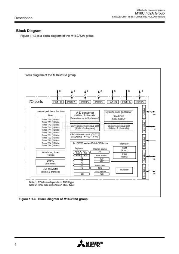
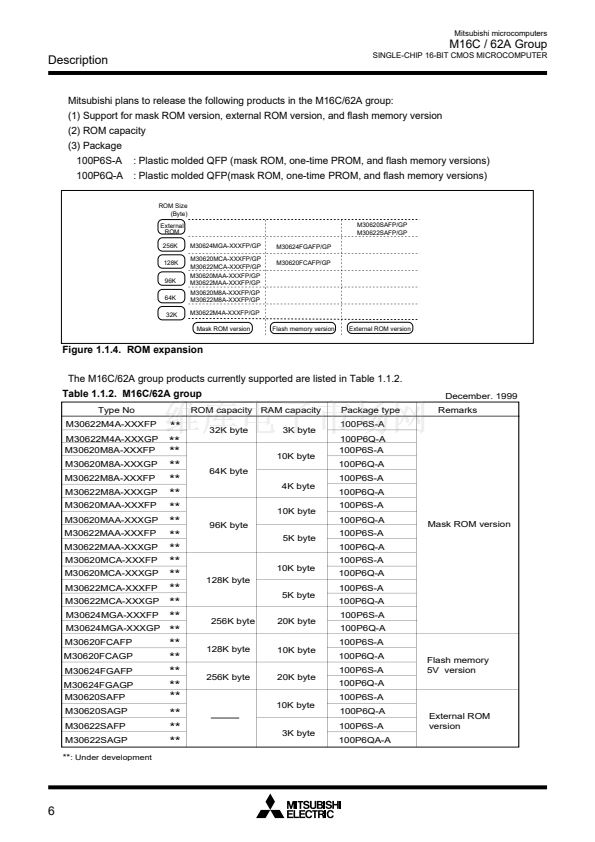
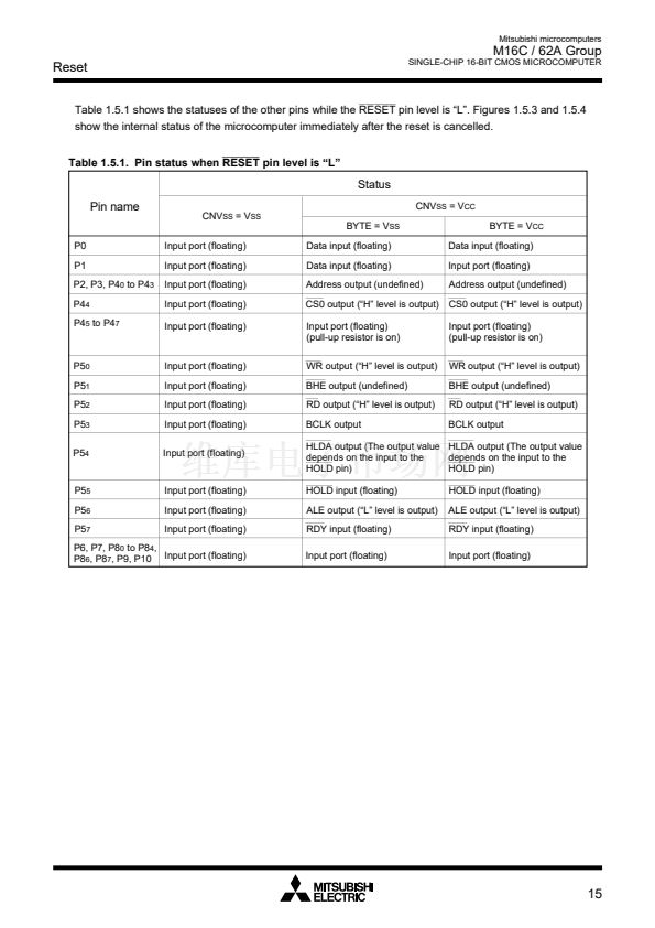
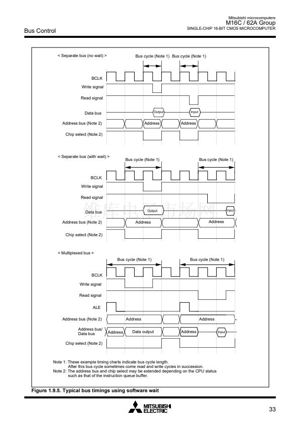
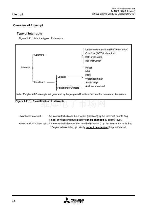
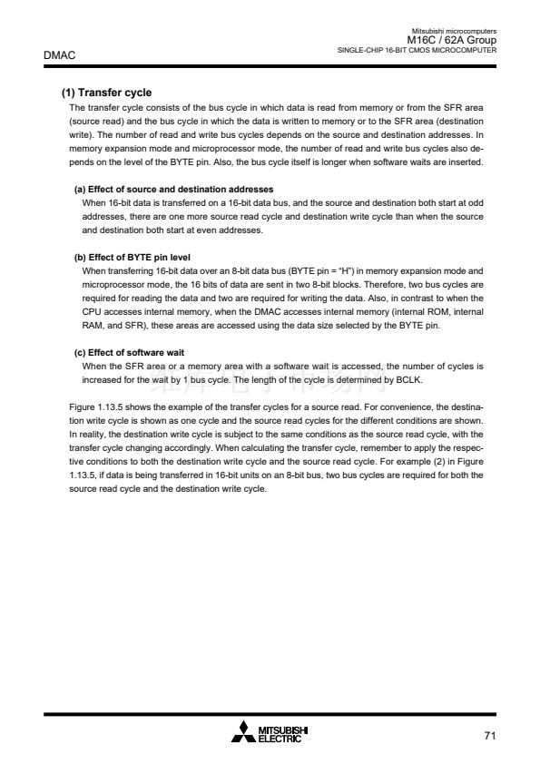
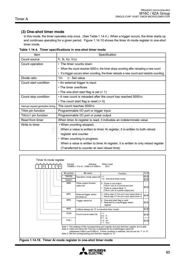
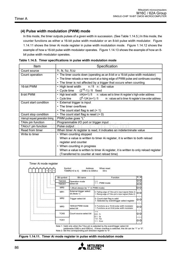
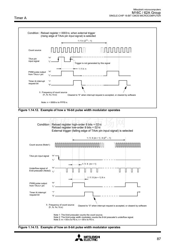
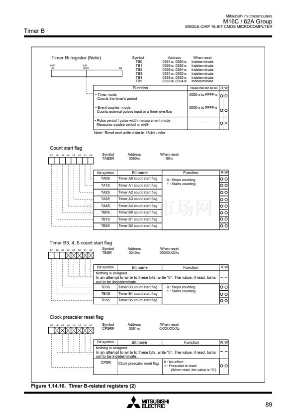
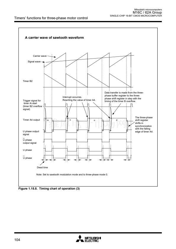
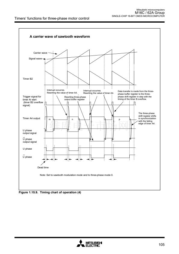
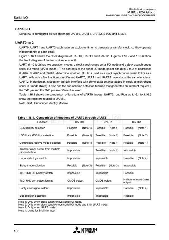
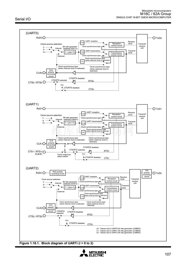
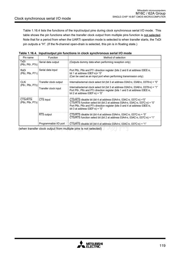
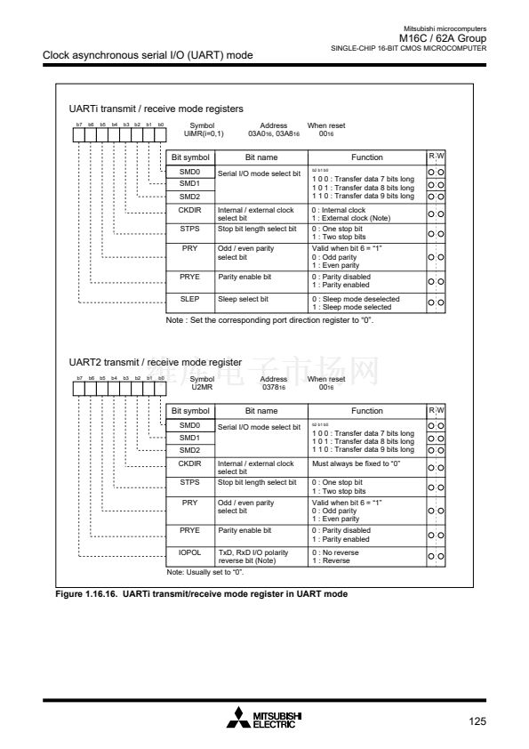
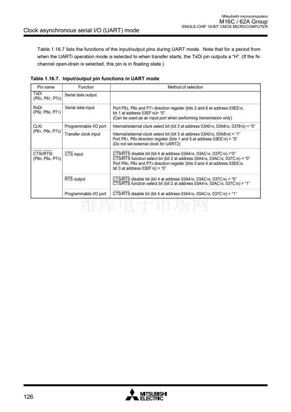
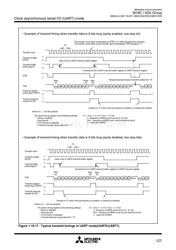
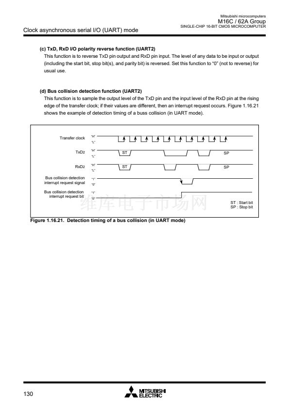
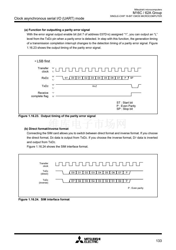
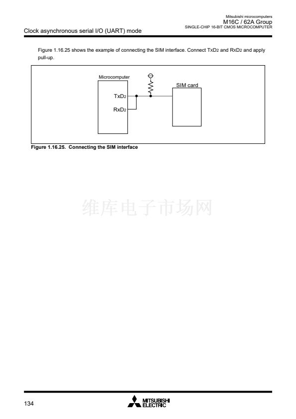
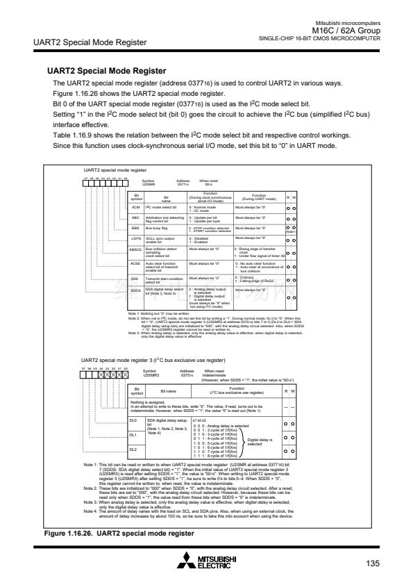
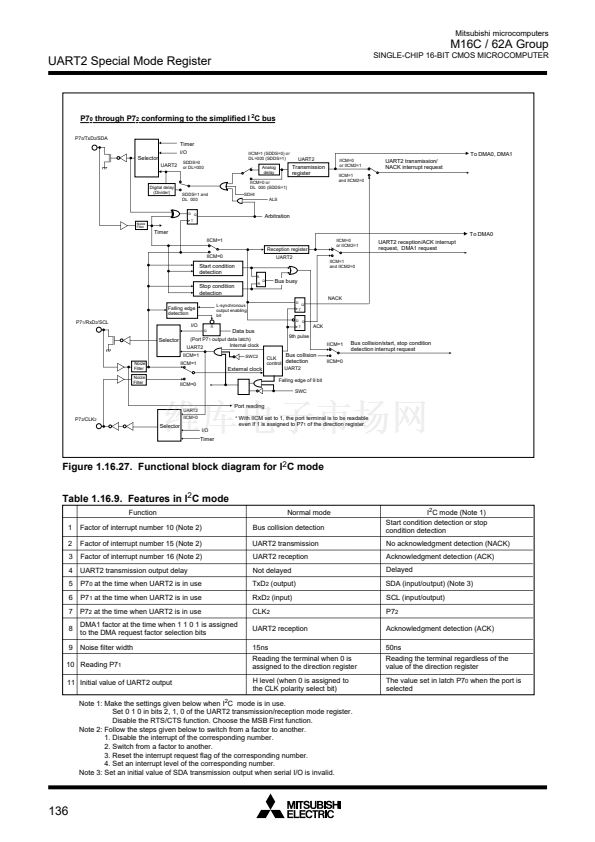
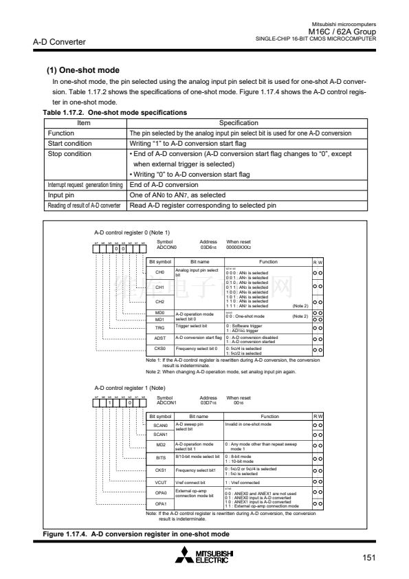
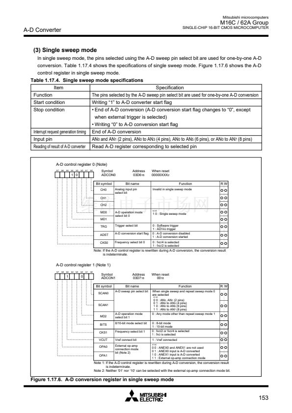
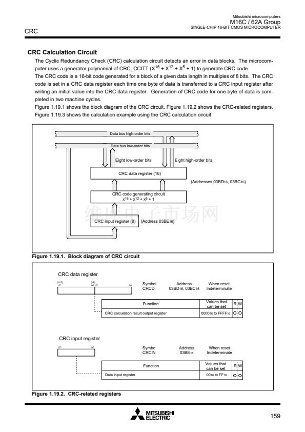
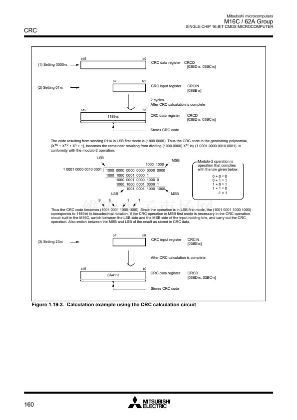
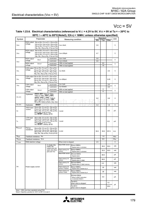
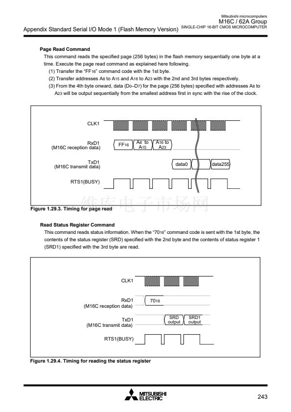
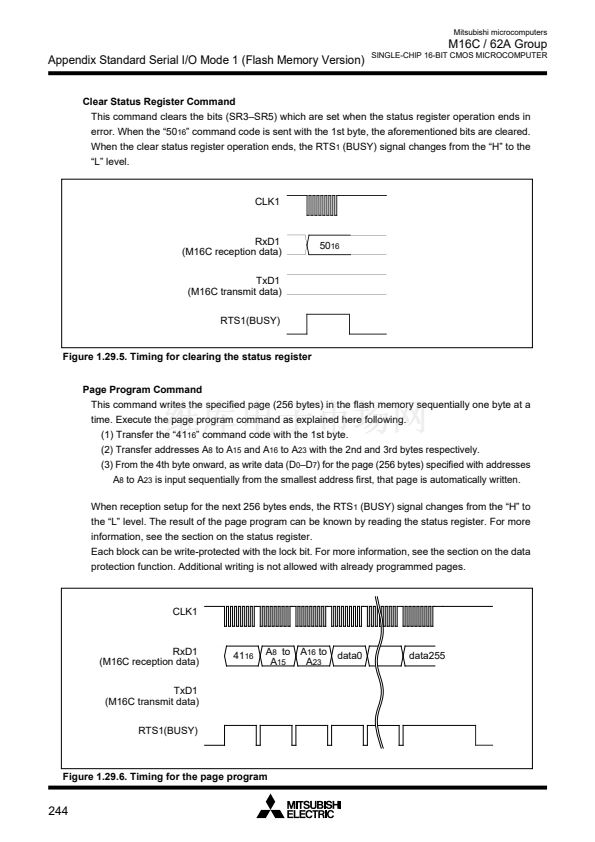
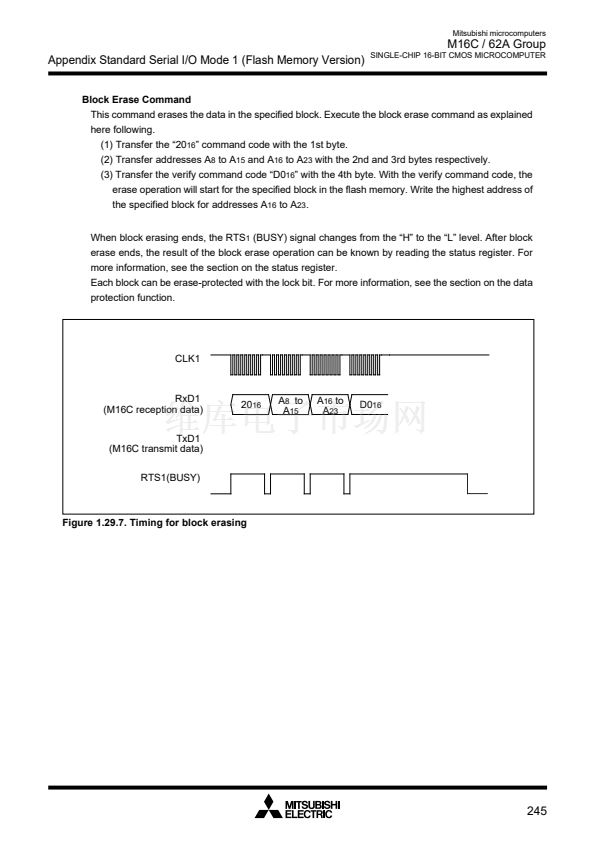
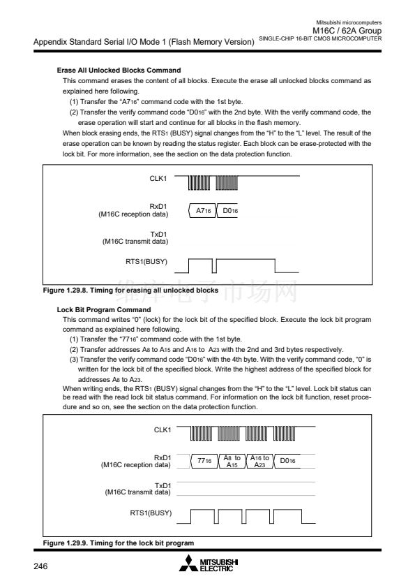
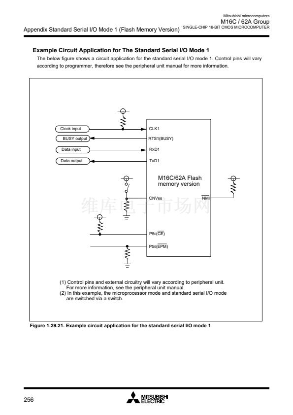
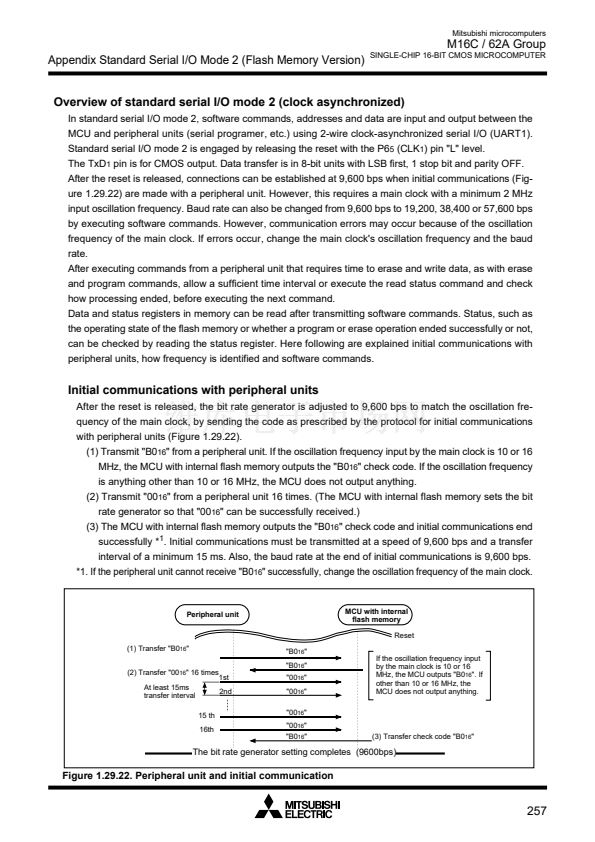
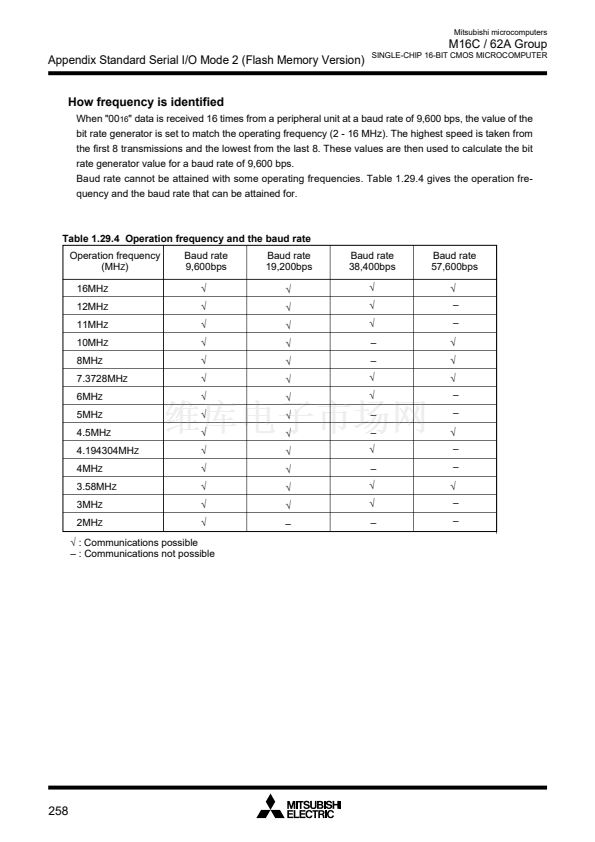
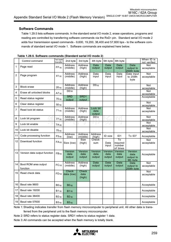
Mitsubishi microcomputers
M16C / 62A Group
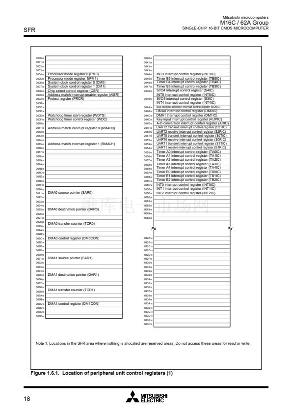
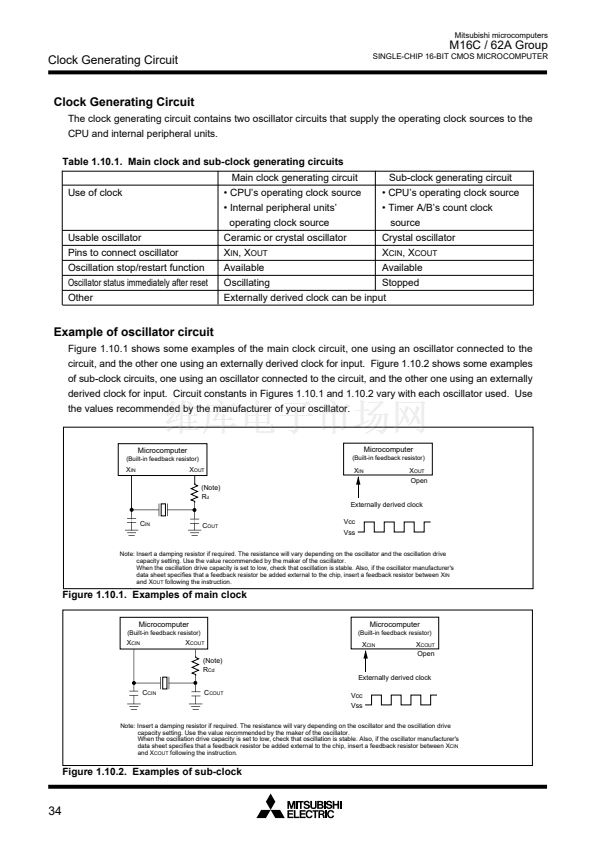
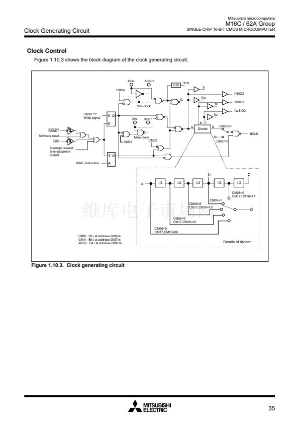
Clock Generating Circuit
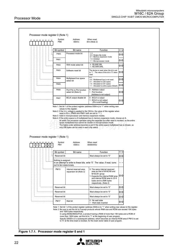
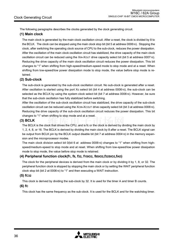
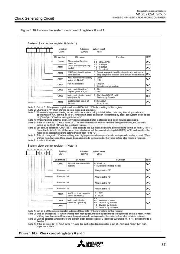
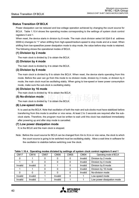
Figure 1.10.4 shows the system clock control registers 0 and 1.
SINGLE-CHIP 16-BIT CMOS MICROCOMPUTER
System clock control register 0 (Note 1)
b7
b6
b5
b4
b3
b2
b1
b0
Symbol
CM0
Bit symbol
CM00
CM01
CM02
CM03
CM04
CM05
CM06
CM07
Address
0006
16
Bit name
Clock output function
select bit
(Valid only in single-chip
mode)
WAIT peripheral function
clock stop bit
When reset
48
16
Function
b1 b0
RW
0 0 : I/O port P5
7
0 1 : f
C
output
1 0 : f
8
output
1 1 : f
32
output
0 : Do not stop peripheral function clock in wait mode
1 : Stop peripheral function clock in wait mode (Note 8)
X
CIN
-X
COUT
drive capacity 0 : LOW
select bit (Note 2)
1 : HIGH
Port X
C
select bit
Main clock (X
IN
-X
OUT
)
stop bit (Note 3, 4, 5)
Main clock division select
bit 0 (Note 7)
System clock select bit
(Note 6)
0 : I/O port
1 : X
CIN
-X
COUT
generation
0 : On
1 : Off
0 : CM16 and CM17 valid
1 : Division by 8 mode
0 : X
IN
, X
OUT
1 : X
CIN
, X
COUT
Note 1: Set bit 0 of the protect register (address 000A
16
) to 鈥?鈥?before writing to this register.
Note 2: Changes to 鈥?鈥?when shiffing to stop mode and at a reset.
Note 3: When entering power saving mode, main clock stops using this bit. When returning from stop mode and
operating with X
IN
, set this bit to 鈥?鈥? When main clock oscillation is operating by itself, set system clock select
bit (CM07) to 鈥?鈥?before setting this bit to 鈥?鈥?
Note 4: When inputting external clock, only clock oscillation buffer is stopped and clock input is acceptable.
Note 5: If this bit is set to 鈥?鈥? X
OUT
turns 鈥淗鈥? The built-in feedback resistor remains being connected, so X
IN
turns
pulled up to X
OUT
(鈥淗鈥? via the feedback resistor.
Note 6: Set port Xc select bit (CM04) to 鈥?鈥?and stabilize the sub-clock oscillating before setting to this bit from 鈥?鈥?to 鈥?鈥?
Do not write to both bits at the same time. And also, set the main clock stop bit (CM05) to 鈥?鈥?and stabilize the
main clock oscillating before setting this bit from 鈥?鈥?to 鈥?鈥?
Note 7: This bit changes to 鈥?鈥?when shifting from high-speed/medium-speed mode to stop mode and at a reset. When
shifting from low-speed/low power dissipation mode to stop mode, the value before stop mode is retained.
Note 8: f
C32
is not included.
System clock control register 1 (Note 1)
b7
b6
b5
b4
b3
b2
b1
b0
0 0
0
0
Symbol
CM1
Bit symbol
CM10
Address
0007
16
Bit name
All clock stop control bit
(Note4)
When reset
20
16
Function
0 : Clock on
1 : All clocks off (stop mode)
Always set to
鈥?鈥?/div>
Always set to
鈥?鈥?/div>
Always set to
鈥?鈥?/div>
Always set to
鈥?鈥?/div>
0 : LOW
1 : HIGH
b7 b6
RW
Reserved bit
Reserved bit
Reserved bit
Reserved bit
CM15
CM16
CM17
X
IN
-X
OUT
drive capacity
select bit (Note 2)
Main clock division
select bit 1 (Note 3)
0 0 : No division mode
0 1 : Division by 2 mode
1 0 : Division by 4 mode
1 1 : Division by 16 mode
Note 1: Set bit 0 of the protect register (address 000A
16
) to 鈥?鈥?before writing to this register.
Note 2: This bit changes to 鈥?鈥?when shifting from high-speed/medium-speed mode to stop mode and at a reset. When
shifting from low-speed/low power dissipation mode to stop mode, the value before stop mode is retained.
Note 3: Can be selected when bit 6 of the system clock control register 0 (address 0006
16
) is 鈥?鈥? If 鈥?鈥? division mode is
fixed at 8.
Note 4: If this bit is set to 鈥?鈥? X
OUT
turns 鈥淗鈥? and the built-in feedback resistor is cut off. X
CIN
and X
COUT
turn high-
impedance state.
Figure 1.10.4. Clock control registers 0 and 1
37


 1
1
 2
2
 3
3
 4
4
 5
5
 6
6
 7
7
 8
8
 9
9
 10
10
 11
11
 12
12
 13
13
 14
14
 15
15
 16
16
 17
17
 18
18
 19
19
 20
20
 21
21
 22
22
 23
23
 24
24
 25
25
 26
26
 27
27
 28
28
 29
29
 30
30
 31
31
 32
32
 33
33
 34
34
 35
35
 36
36
 37
37
 38
38
 39
39
 40
40
 41
41
 42
42
 43
43
 44
44
 45
45
 46
46
 47
47
 48
48
 49
49
 50
50
 51
51
 52
52
 53
53
 54
54
 55
55
 56
56
 57
57
 58
58
 59
59
 60
60
 61
61
 62
62
 63
63
 64
64
 65
65
 66
66
 67
67
 68
68
 69
69
 70
70
 71
71
 72
72
 73
73
 74
74
 75
75
 76
76
 77
77
 78
78
 79
79
 80
80
 81
81
 82
82
 83
83
 84
84
 85
85
 86
86
 87
87
 88
88
 89
89
 90
90
 91
91
 92
92
 93
93
 94
94
 95
95
 96
96
 97
97
 98
98
 99
99
 100
100
 101
101
 102
102
 103
103
 104
104
 105
105
 106
106
 107
107
 108
108
 109
109
 110
110
 111
111
 112
112
 113
113
 114
114
 115
115
 116
116
 117
117
 118
118
 119
119
 120
120
 121
121
 122
122
 123
123
 124
124
 125
125
 126
126
 127
127
 128
128
 129
129
 130
130
 131
131
 132
132
 133
133
 134
134
 135
135
 136
136
 137
137
 138
138
 139
139
 140
140
 141
141
 142
142
 143
143
 144
144
 145
145
 146
146
 147
147
 148
148
 149
149
 150
150
 151
151
 152
152
 153
153
 154
154
 155
155
 156
156
 157
157
 158
158
 159
159
 160
160
 161
161
 162
162
 163
163
 164
164
 165
165
 166
166
 167
167
 168
168
 169
169
 170
170
 171
171
 172
172
 173
173
 174
174
 175
175
 176
176
 177
177
 178
178
 179
179
 180
180
 181
181
 182
182
 183
183
 184
184
 185
185
 186
186
 187
187
 188
188
 189
189
 190
190
 191
191
 192
192
 193
193
 194
194
 195
195
 196
196
 197
197
 198
198
 199
199
 200
200
 201
201
 202
202
 203
203
 204
204
 205
205
 206
206
 207
207
 208
208
 209
209
 210
210
 211
211
 212
212
 213
213
 214
214
 215
215
 216
216
 217
217
 218
218
 219
219
 220
220
 221
221
 222
222
 223
223
 224
224
 225
225
 226
226
 227
227
 228
228
 229
229
 230
230
 231
231
 232
232
 233
233
 234
234
 235
235
 236
236
 237
237
 238
238
 239
239
 240
240
 241
241
 242
242
 243
243
 244
244
 245
245
 246
246
 247
247
 248
248
 249
249
 250
250
 251
251
 252
252
 253
253
 254
254
 255
255
 256
256
 257
257
 258
258
 259
259
 260
260
 261
261
 262
262
 263
263
 264
264
 265
265
 266
266
 267
267
 268
268
 269
269
 270
270
 271
271
 272
272
 273
273
 274
274
