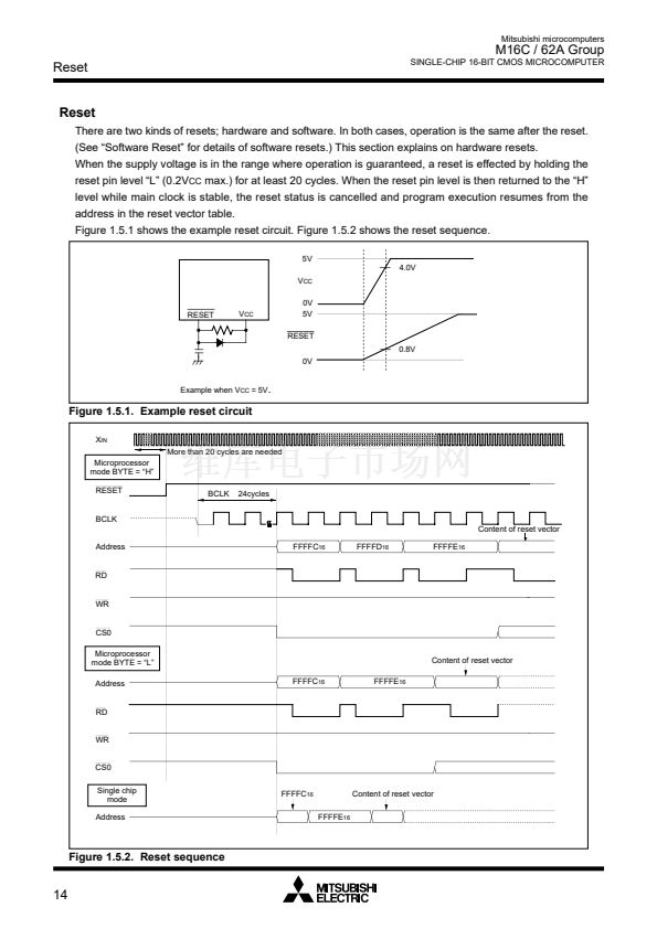
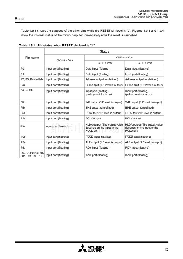
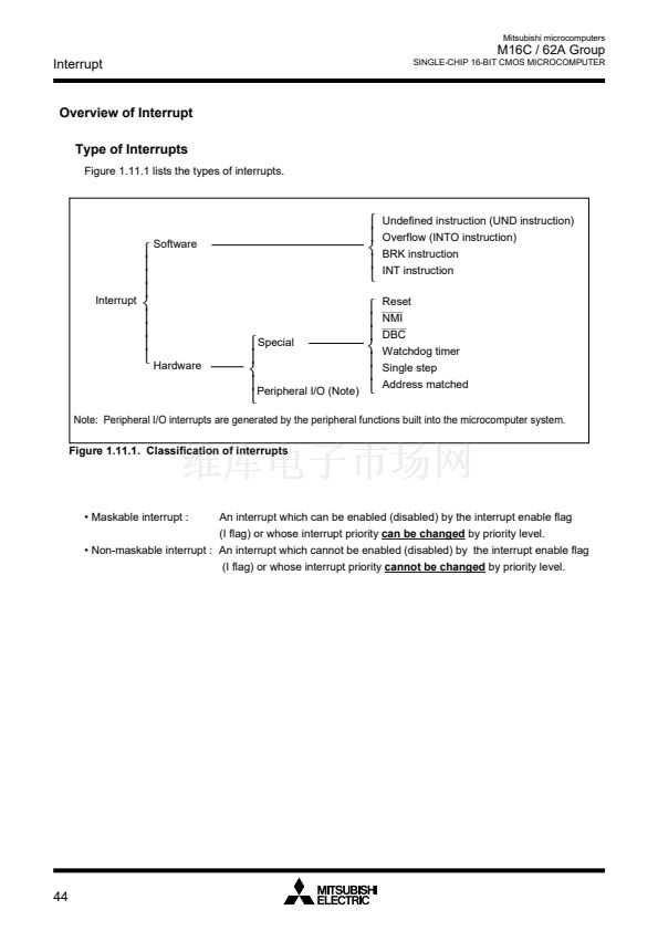
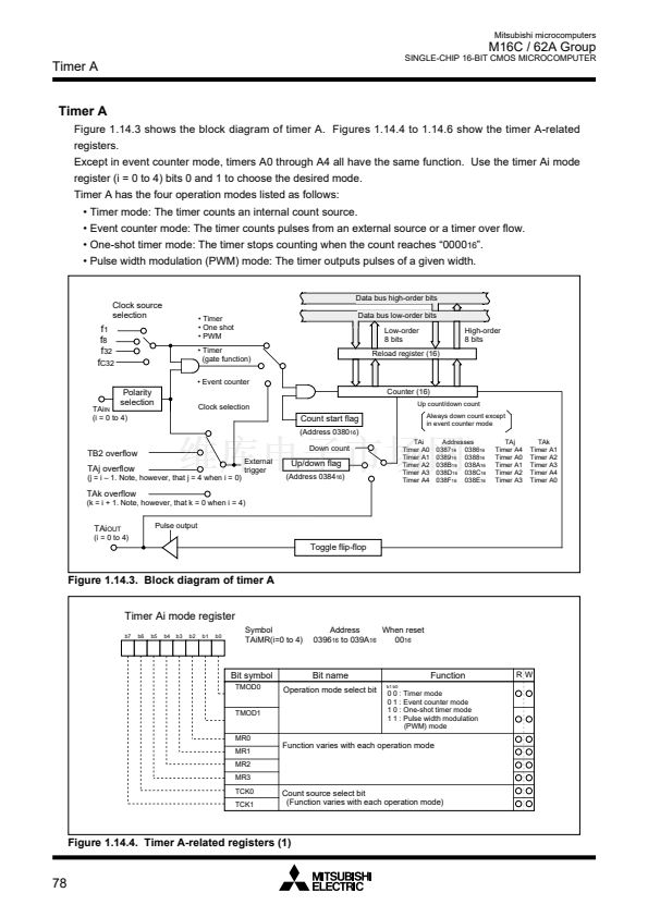
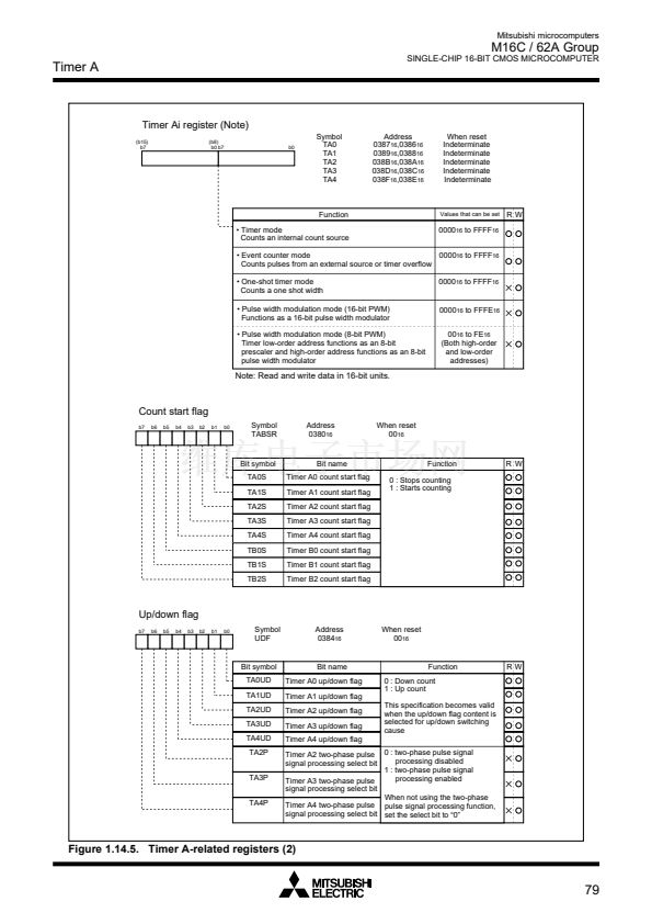
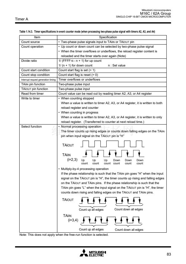
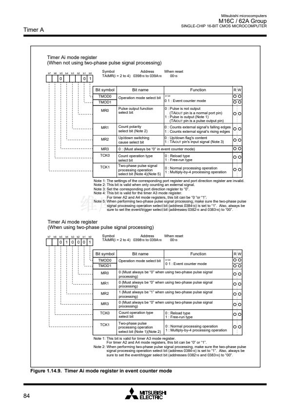
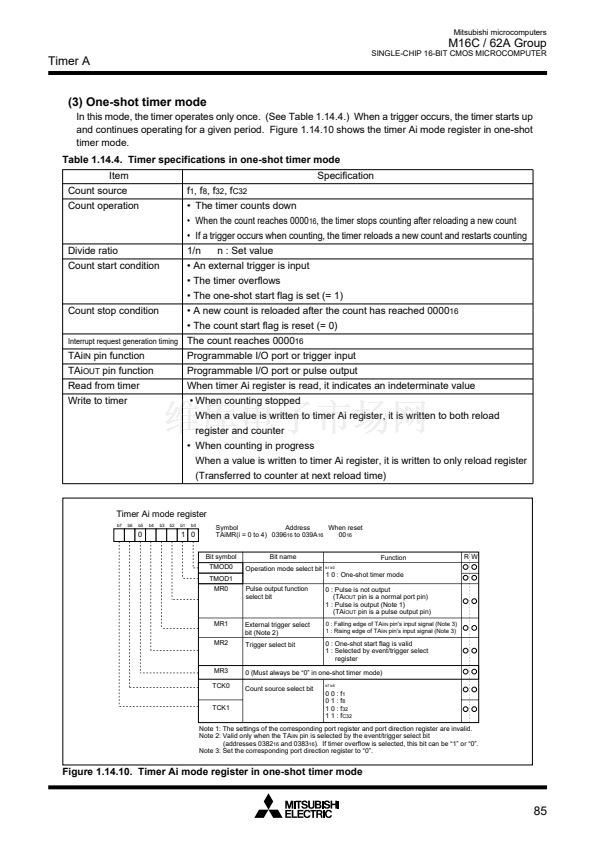
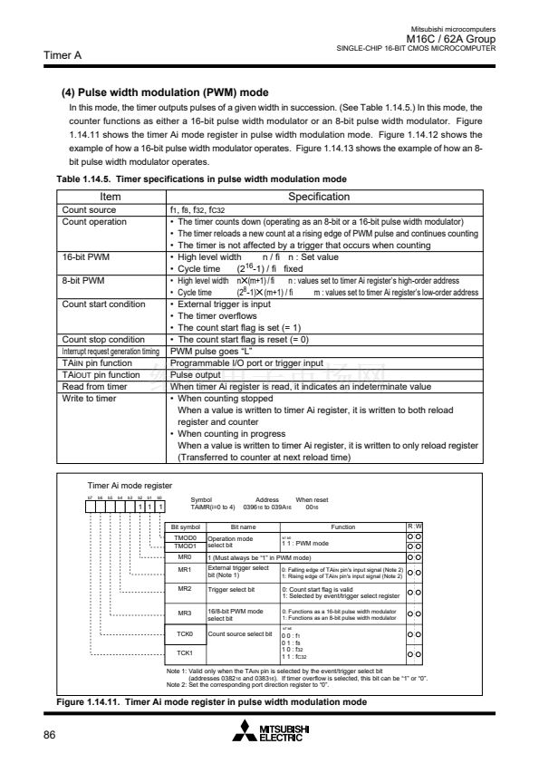
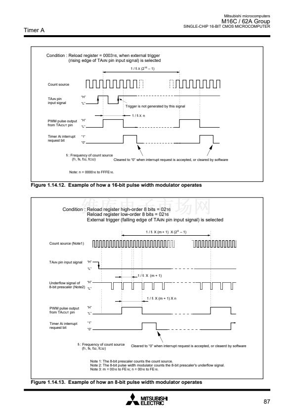
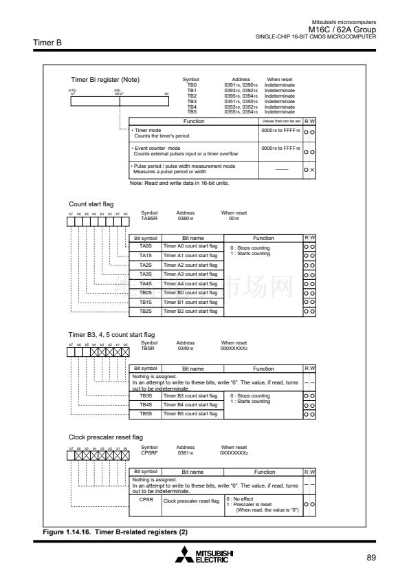
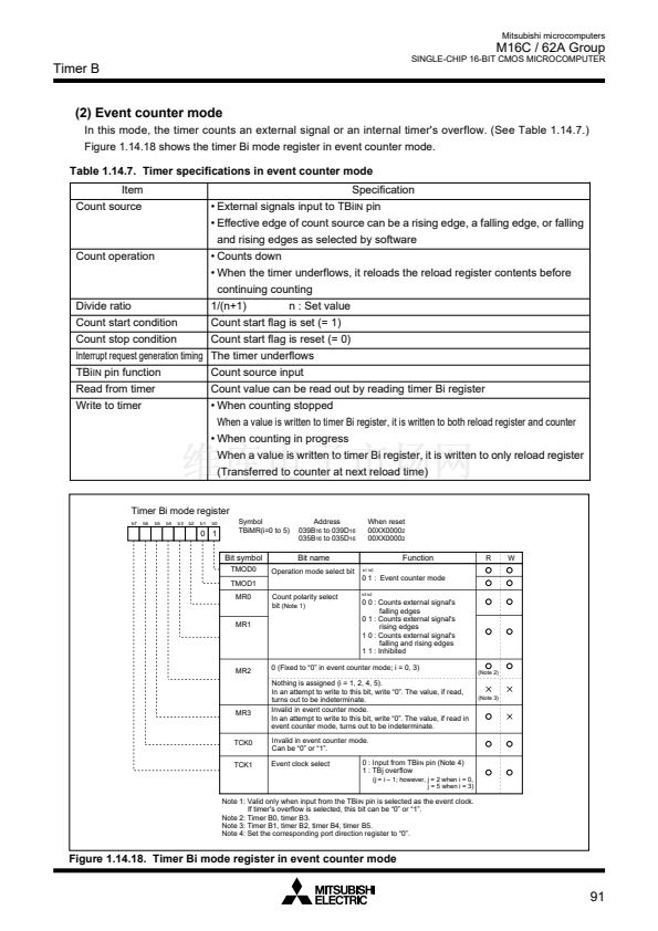
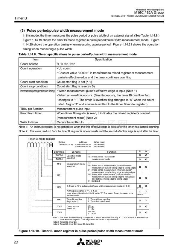
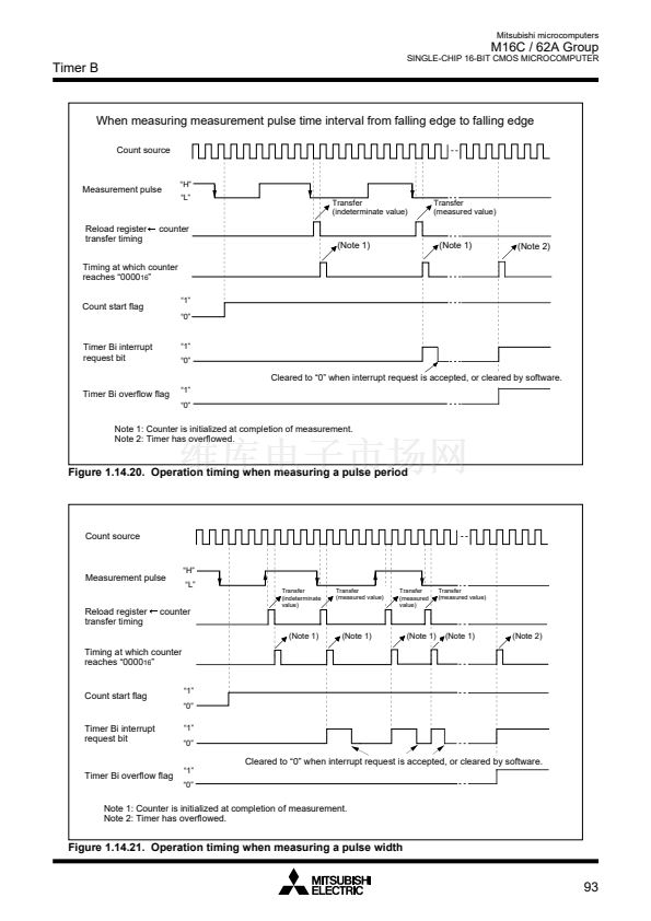
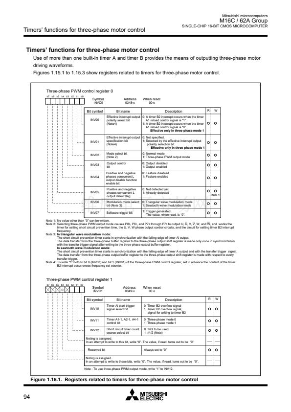
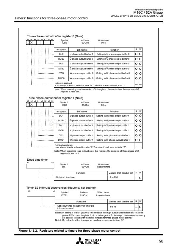
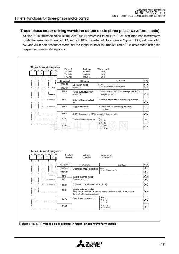
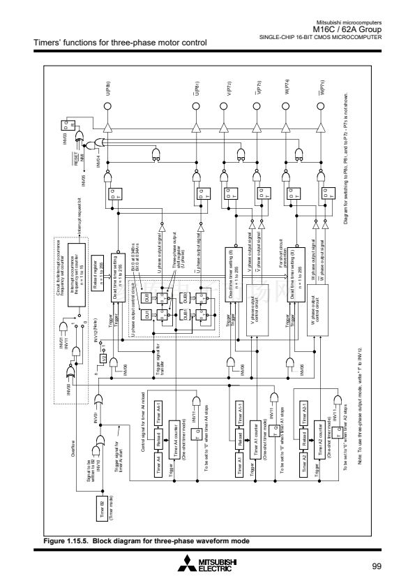
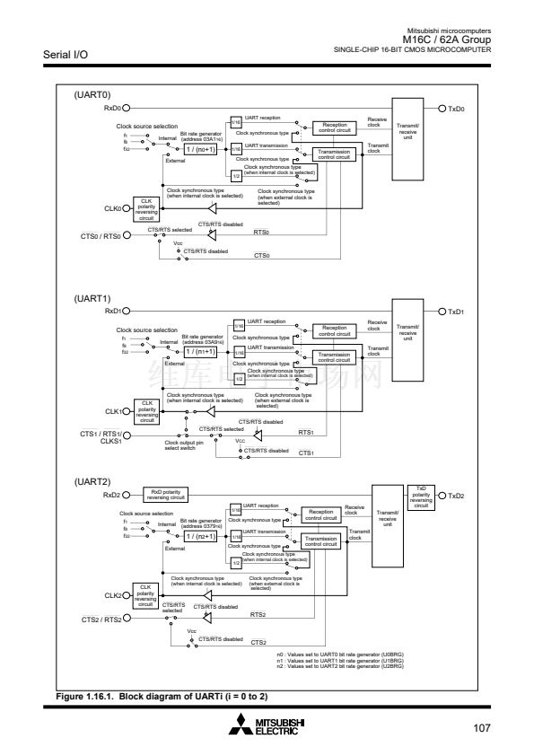
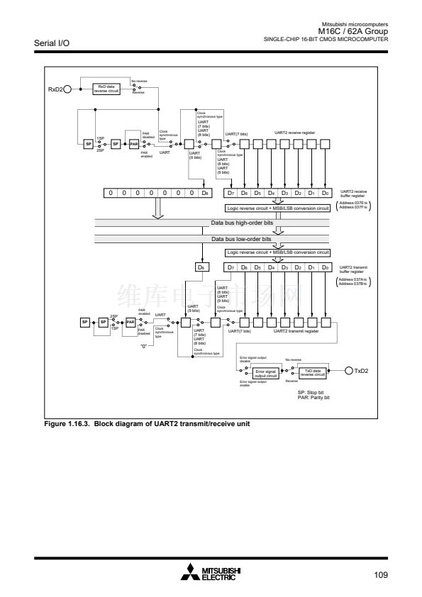
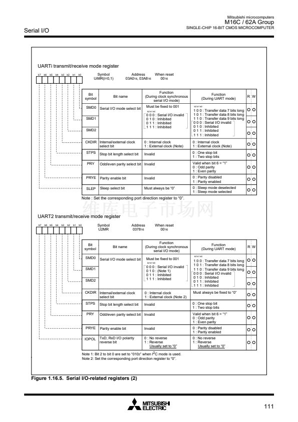
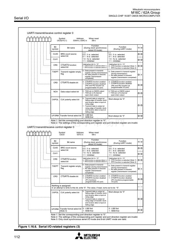
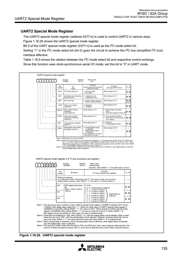
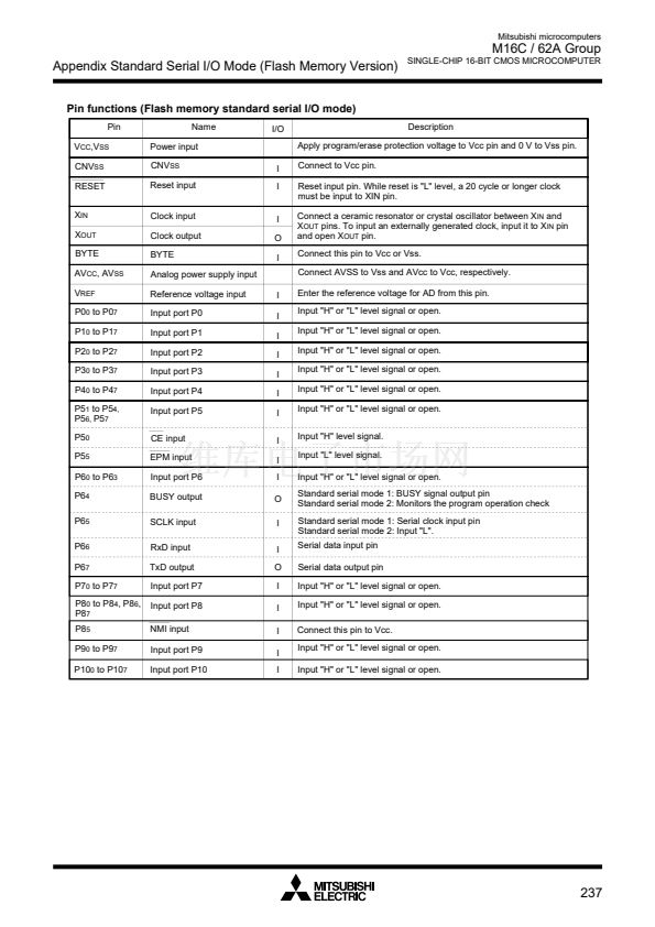
Mitsubishi microcomputers
M16C / 62A Group
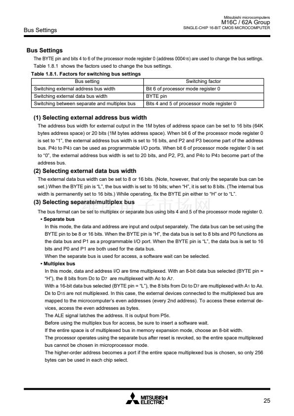
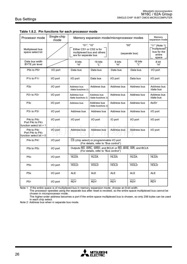
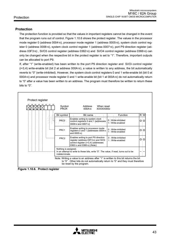
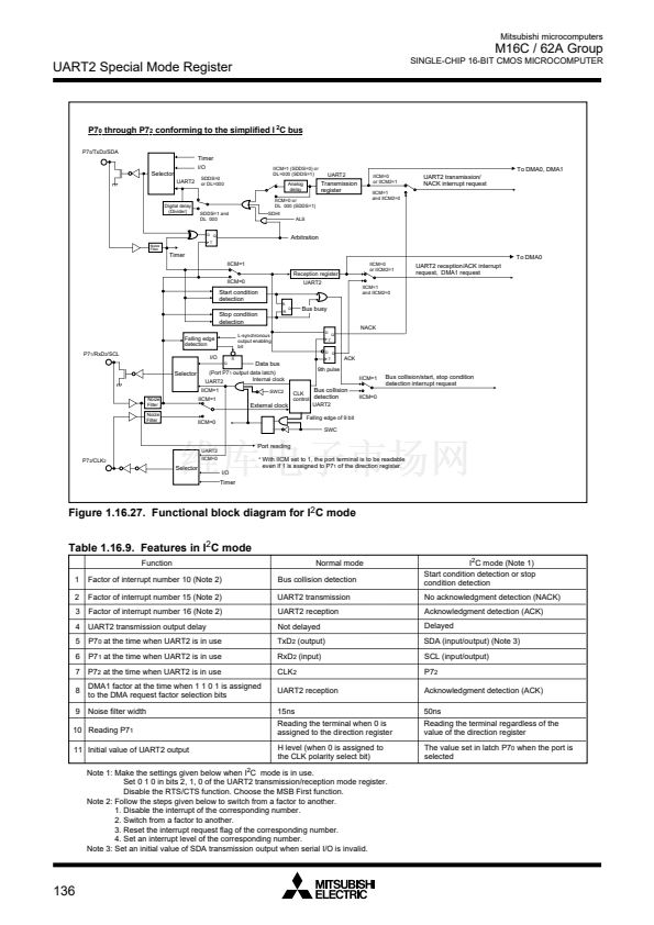
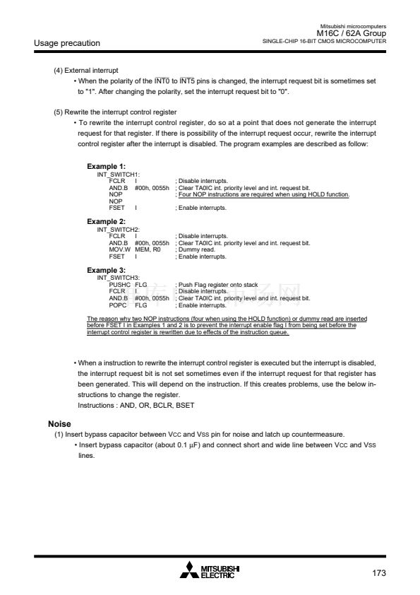
Bus Settings
Bus Settings
SINGLE-CHIP 16-BIT CMOS MICROCOMPUTER
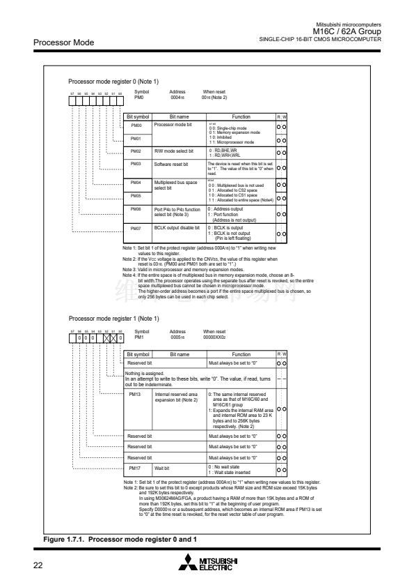
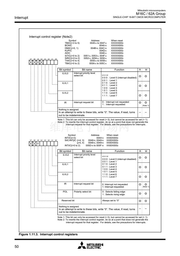
The BYTE pin and bits 4 to 6 of the processor mode register 0 (address 0004
16
) are used to change the bus settings.
Table 1.8.1 shows the factors used to change the bus settings.
Table 1.8.1. Factors for switching bus settings
Bus setting
Switching external address bus width
Switching external data bus width
Switching between separate and multiplex bus
Switching factor
Bit 6 of processor mode register 0
BYTE pin
Bits 4 and 5 of processor mode register 0
(1) Selecting external address bus width
The address bus width for external output in the 1M bytes of address space can be set to 16 bits (64K
bytes address space) or 20 bits (1M bytes address space). When bit 6 of the processor mode register 0
is set to 鈥?鈥? the external address bus width is set to 16 bits, and P2 and P3 become part of the address
bus. P4
0
to P4
3
can be used as programmable I/O ports. When bit 6 of processor mode register 0 is set
to 鈥?鈥? the external address bus width is set to 20 bits, and P2, P3, and P4
0
to P4
3
become part of the
address bus.
(2) Selecting external data bus width
The external data bus width can be set to 8 or 16 bits. (Note, however, that only the separate bus can be
set.) When the BYTE pin is 鈥淟鈥? the bus width is set to 16 bits; when 鈥淗鈥? it is set to 8 bits. (The internal bus
width is permanently set to 16 bits.) While operating, fix the BYTE pin either to 鈥淗鈥?or to 鈥淟鈥?
(3) Selecting separate/multiplex bus
The bus format can be set to multiplex or separate bus using bits 4 and 5 of the processor mode register 0.
鈥?Separate bus
In this mode, the data and address are input and output separately. The data bus can be set using the
BYTE pin to be 8 or 16 bits. When the BYTE pin is 鈥淗鈥? the data bus is set to 8 bits and P0 functions as
the data bus and P1 as a programmable I/O port. When the BYTE pin is 鈥淟鈥? the data bus is set to 16
bits and P0 and P1 are both used for the data bus.
When the separate bus is used for access, a software wait can be selected.
鈥?Multiplex bus
In this mode, data and address I/O are time multiplexed. With an 8-bit data bus selected (BYTE pin =
鈥淗鈥?, the 8 bits from D
0
to D
7
are multiplexed with A
0
to A
7
.
With a 16-bit data bus selected (BYTE pin = 鈥淟鈥?, the 8 bits from D
0
to D
7
are multiplexed with A
1
to A
8
.
D
8
to D
15
are not multiplexed. In this case, the external devices connected to the multiplexed bus are
mapped to the microcomputer鈥檚 even addresses (every 2nd address). To access these external de-
vices, access the even addresses as bytes.
The ALE signal latches the address. It is output from P5
6
.
Before using the multiplex bus for access, be sure to insert a software wait.
If the entire space is of multiplexed bus in memory expansion mode, choose an 8-bit width.
The processor operates using the separate bus after reset is revoked, so the entire space multiplexed
bus cannot be chosen in microprocessor mode.
The higher-order address becomes a port if the entire space multiplexed bus is chosen, so only 256
bytes can be used in each chip select.
25


 1
1
 2
2
 3
3
 4
4
 5
5
 6
6
 7
7
 8
8
 9
9
 10
10
 11
11
 12
12
 13
13
 14
14
 15
15
 16
16
 17
17
 18
18
 19
19
 20
20
 21
21
 22
22
 23
23
 24
24
 25
25
 26
26
 27
27
 28
28
 29
29
 30
30
 31
31
 32
32
 33
33
 34
34
 35
35
 36
36
 37
37
 38
38
 39
39
 40
40
 41
41
 42
42
 43
43
 44
44
 45
45
 46
46
 47
47
 48
48
 49
49
 50
50
 51
51
 52
52
 53
53
 54
54
 55
55
 56
56
 57
57
 58
58
 59
59
 60
60
 61
61
 62
62
 63
63
 64
64
 65
65
 66
66
 67
67
 68
68
 69
69
 70
70
 71
71
 72
72
 73
73
 74
74
 75
75
 76
76
 77
77
 78
78
 79
79
 80
80
 81
81
 82
82
 83
83
 84
84
 85
85
 86
86
 87
87
 88
88
 89
89
 90
90
 91
91
 92
92
 93
93
 94
94
 95
95
 96
96
 97
97
 98
98
 99
99
 100
100
 101
101
 102
102
 103
103
 104
104
 105
105
 106
106
 107
107
 108
108
 109
109
 110
110
 111
111
 112
112
 113
113
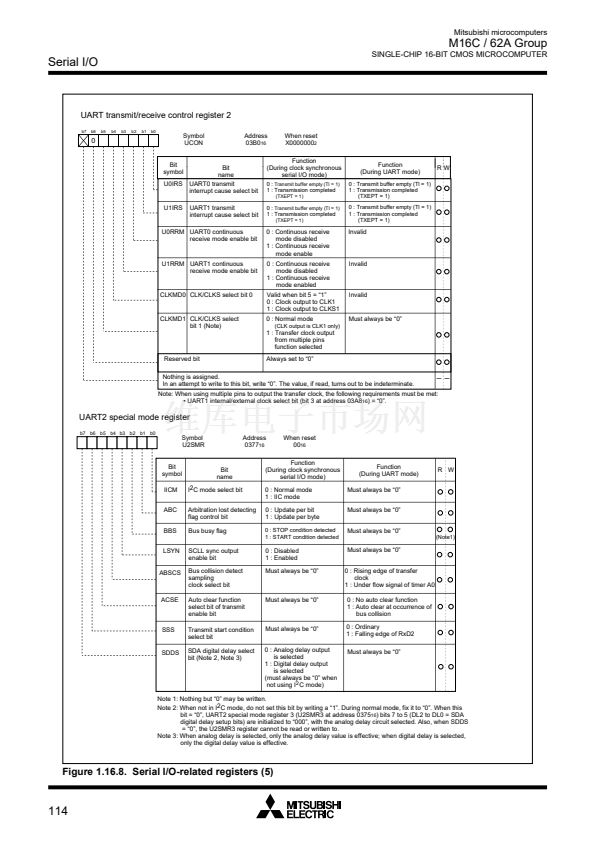 114
114
 115
115
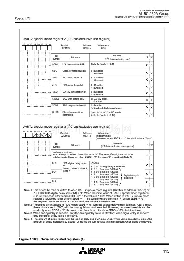
 116
116
 117
117
 118
118
 119
119
 120
120
 121
121
 122
122
 123
123
 124
124
 125
125
 126
126
 127
127
 128
128
 129
129
 130
130
 131
131
 132
132
 133
133
 134
134
 135
135
 136
136
 137
137
 138
138
 139
139
 140
140
 141
141
 142
142
 143
143
 144
144
 145
145
 146
146
 147
147
 148
148
 149
149
 150
150
 151
151
 152
152
 153
153
 154
154
 155
155
 156
156
 157
157
 158
158
 159
159
 160
160
 161
161
 162
162
 163
163
 164
164
 165
165
 166
166
 167
167
 168
168
 169
169
 170
170
 171
171
 172
172
 173
173
 174
174
 175
175
 176
176
 177
177
 178
178
 179
179
 180
180
 181
181
 182
182
 183
183
 184
184
 185
185
 186
186
 187
187
 188
188
 189
189
 190
190
 191
191
 192
192
 193
193
 194
194
 195
195
 196
196
 197
197
 198
198
 199
199
 200
200
 201
201
 202
202
 203
203
 204
204
 205
205
 206
206
 207
207
 208
208
 209
209
 210
210
 211
211
 212
212
 213
213
 214
214
 215
215
 216
216
 217
217
 218
218
 219
219
 220
220
 221
221
 222
222
 223
223
 224
224
 225
225
 226
226
 227
227
 228
228
 229
229
 230
230
 231
231
 232
232
 233
233
 234
234
 235
235
 236
236
 237
237
 238
238
 239
239
 240
240
 241
241
 242
242
 243
243
 244
244
 245
245
 246
246
 247
247
 248
248
 249
249
 250
250
 251
251
 252
252
 253
253
 254
254
 255
255
 256
256
 257
257
 258
258
 259
259
 260
260
 261
261
 262
262
 263
263
 264
264
 265
265
 266
266
 267
267
 268
268
 269
269
 270
270
 271
271
 272
272
 273
273
 274
274
