鈥?/div>
25掳C
(Note 4)
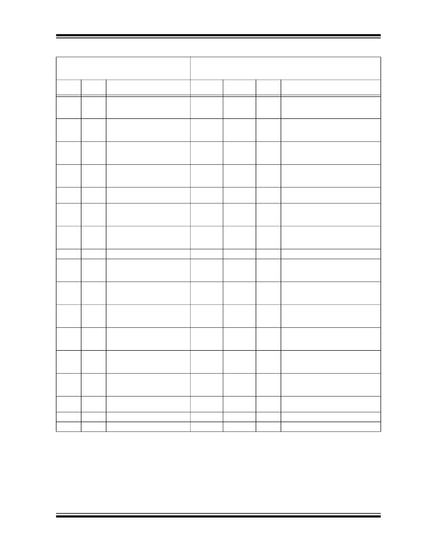
AC CHARACTERISTICS
Param.
No.
Sym
F
CLK
1
2
T
HIGH
Clock high time
ns
3
T
LOW
Clock low time
ns
4
T
R
SDA and SCL rise time
(Note 1)
ns
5
6
T
F
SDA and SCL fall time
(Note 1)
ns
ns
T
HD
:
STA
Start condition hold time
7
T
SU
:
STA
Start condition setup time
ns
8
9
T
HD
:
DAT
Data input hold time
T
SU
:
DAT
Data input setup time
ns
ns
10
T
SU
:
STO
Stop condition setup time
ns
11
T
SU
:
WP
WP setup time
ns
12
T
HD
:
WP
WP hold time
ns
13
T
AA
Output valid from clock
(Note 2)
ns
14
T
BUF
Bus free time: Time the bus must
be free before a new transmis-
sion can start
Input filter spike suppression
(SDA and SCL pins)
Write cycle time (byte or page)
Endurance
ns
16
17
18
Note 1:
2:
3:
4:
T
SP
T
WC
鈥?/div>
ns
ms
cycles
Not 100% tested. C
B
= total capacitance of one bus line in pF.
As a transmitter, the device must provide an internal minimum delay time to bridge the undefined region (minimum
300 ns) of the falling edge of SCL to avoid unintended generation of Start or Stop conditions.
The combined T
SP
and V
HYS
specifications are due to new Schmitt Trigger inputs which provide improved noise spike
suppression. This eliminates the need for a T
I
specification for standard operation.
This parameter is not tested but ensured by characterization. For endurance estimates in a specific application, please
consult the Total Endurance鈩?Model which can be obtained from Microchip鈥檚 web site: www.microchip.com.
铮?/div>
2004 Microchip Technology Inc.
DS21754E-page 3


 1
1
 2
2
 3
3
 4
4
 5
5
 6
6
 7
7
 8
8
 9
9
 10
10
 11
11
 12
12
 13
13
 14
14
 15
15
 16
16
 17
17
 18
18
 19
19
 20
20
 21
21
 22
22
 23
23
 24
24
 25
25
 26
26
