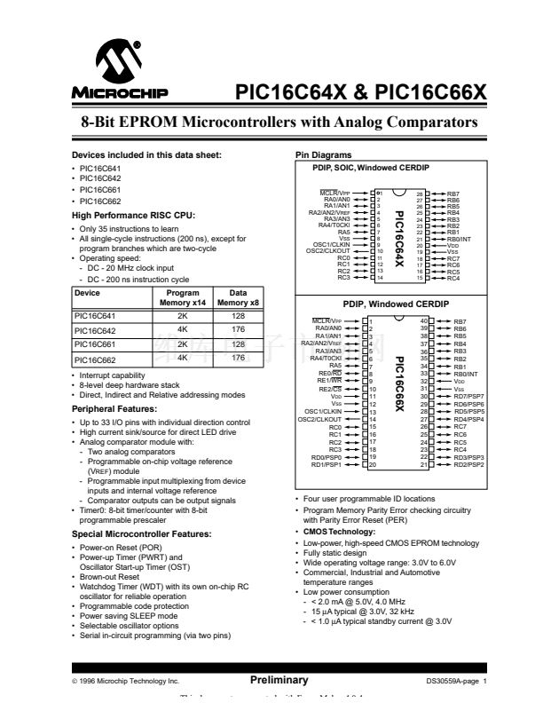
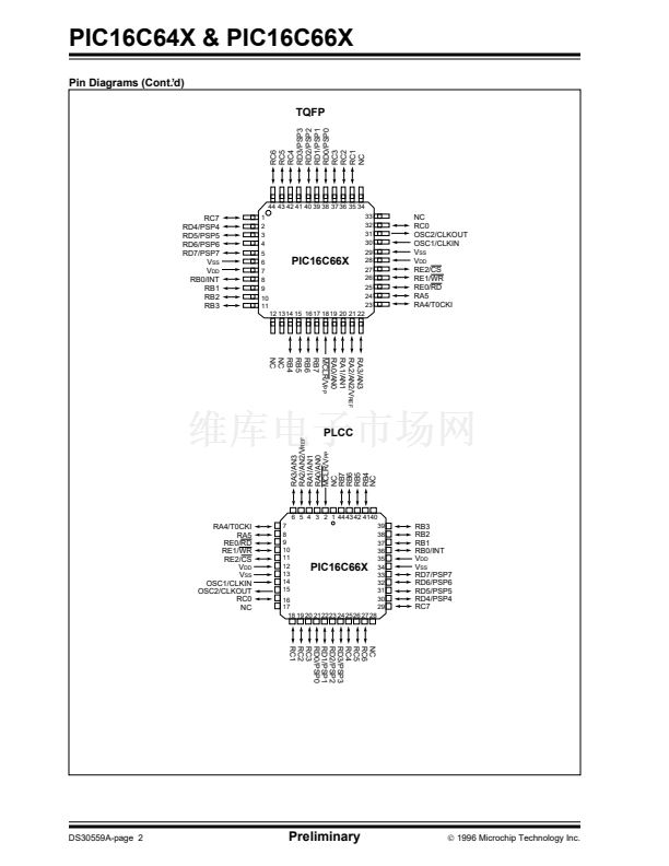
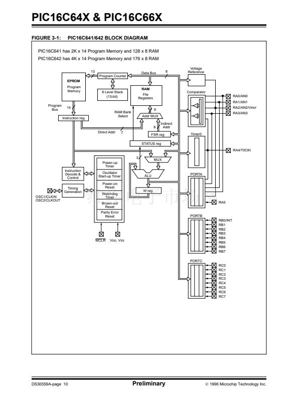
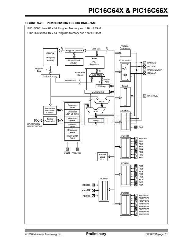
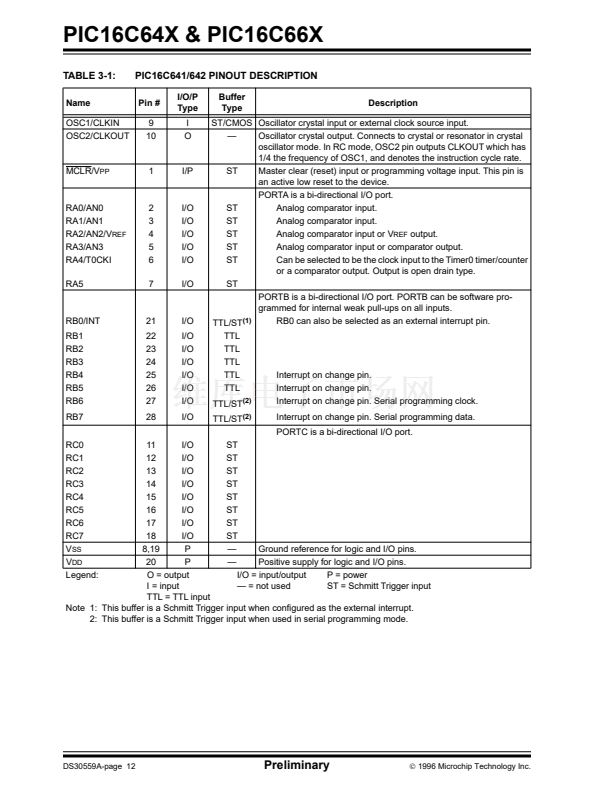
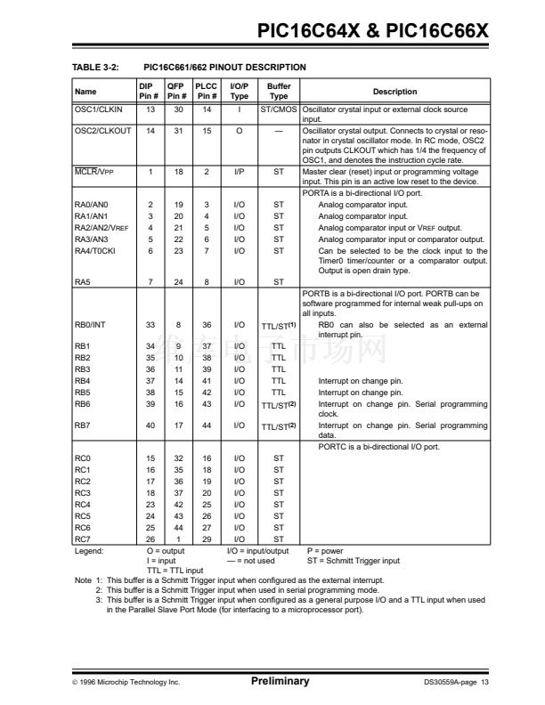
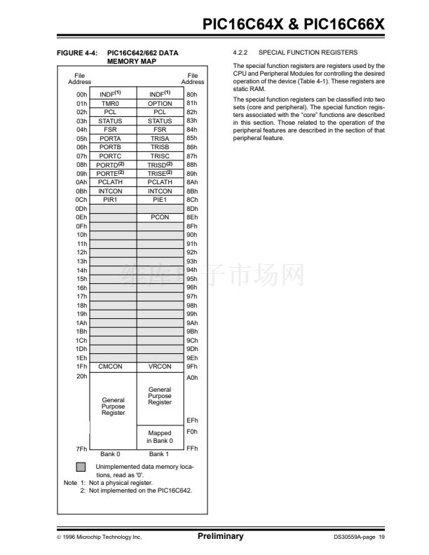
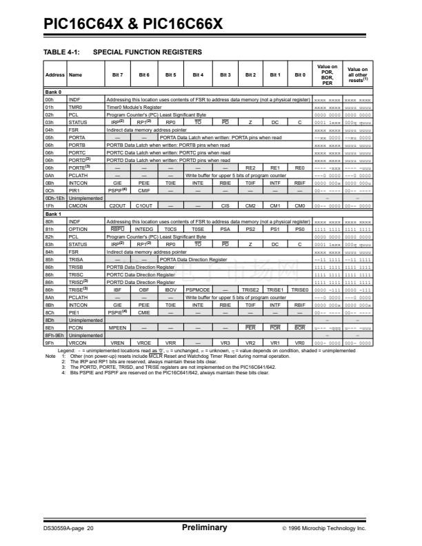
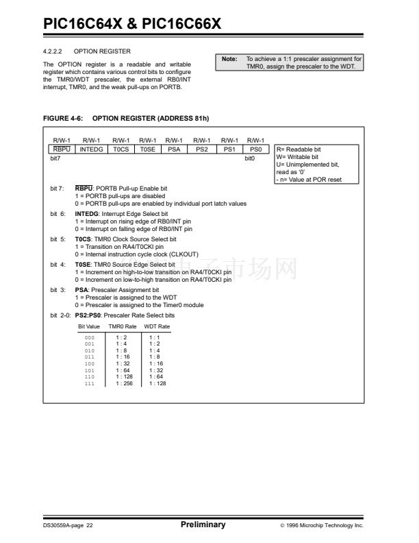
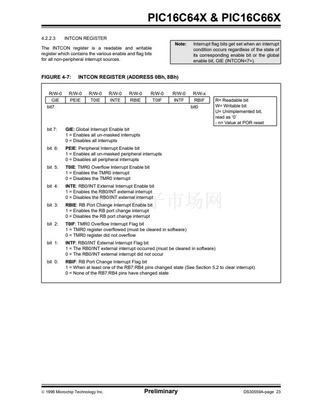
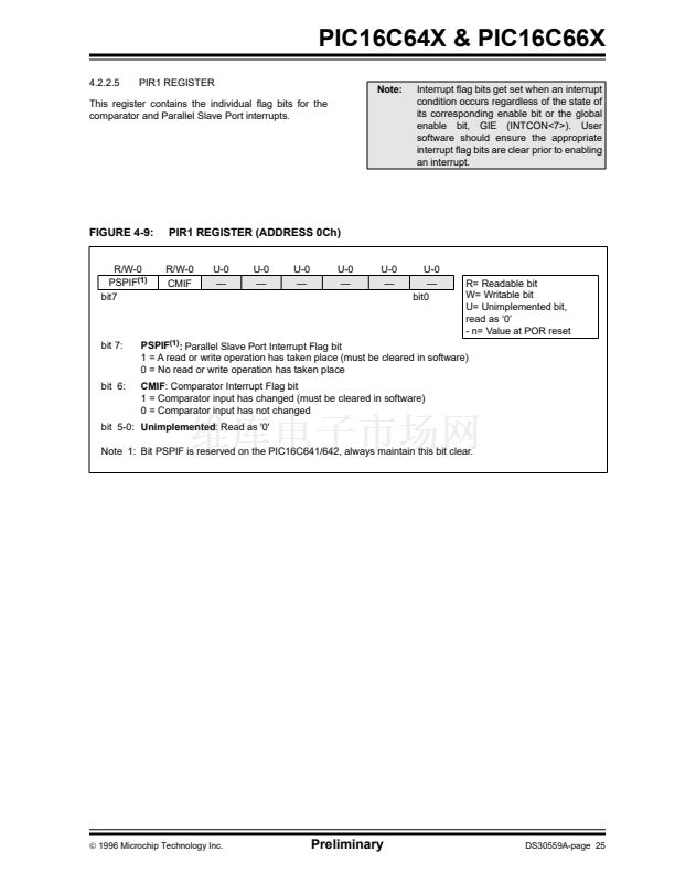
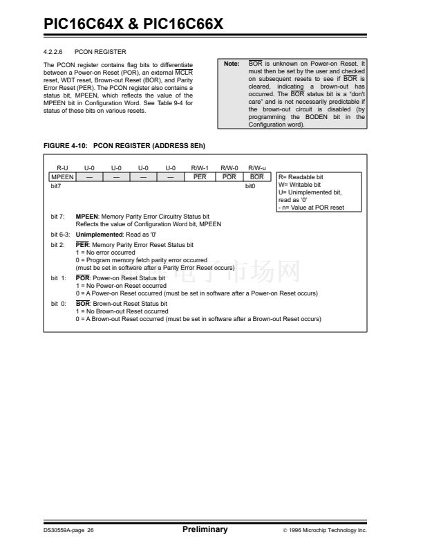
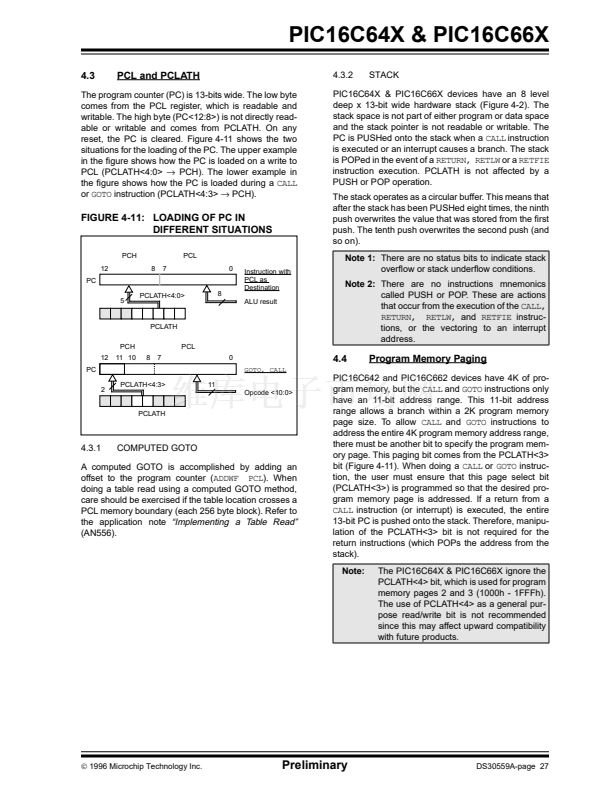
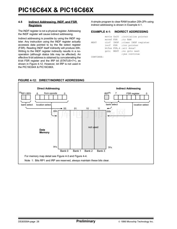
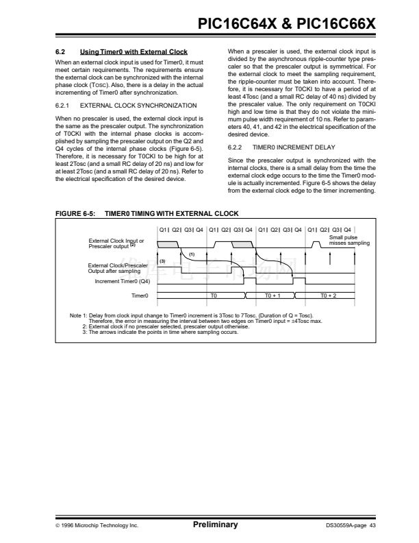
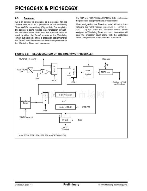
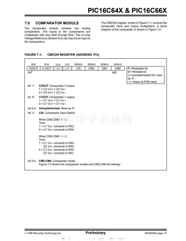
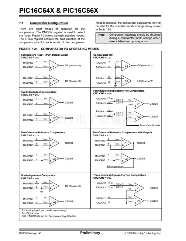
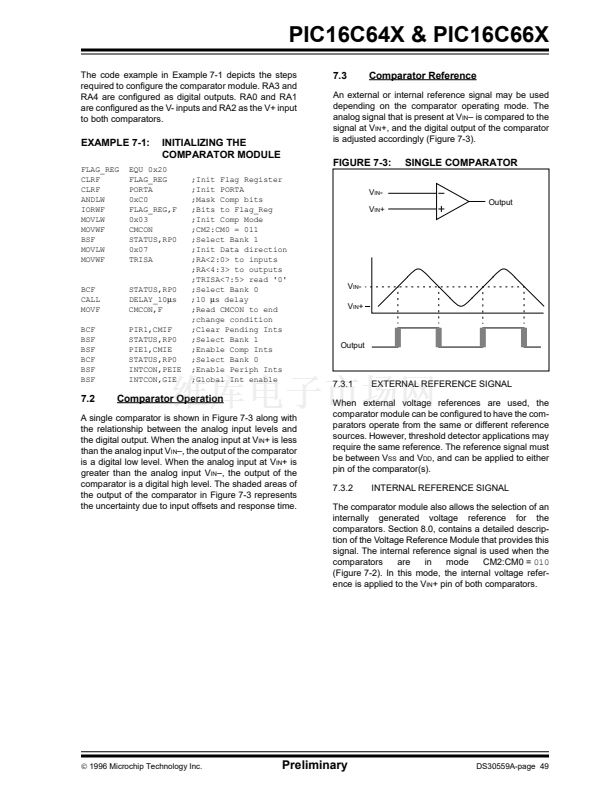
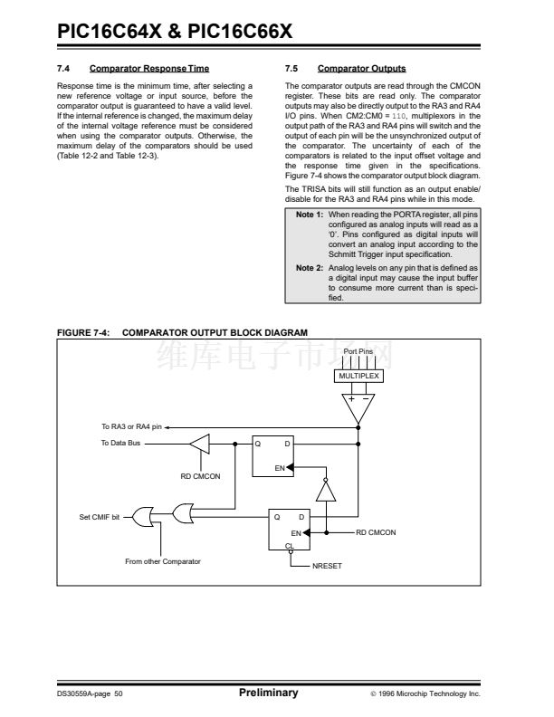
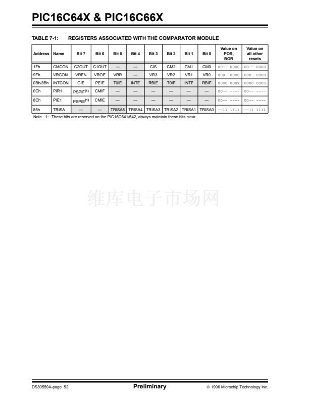
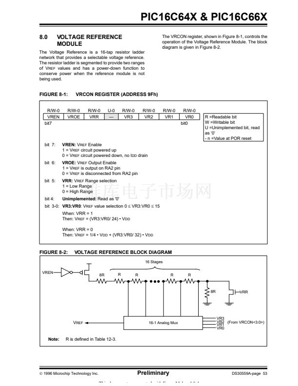
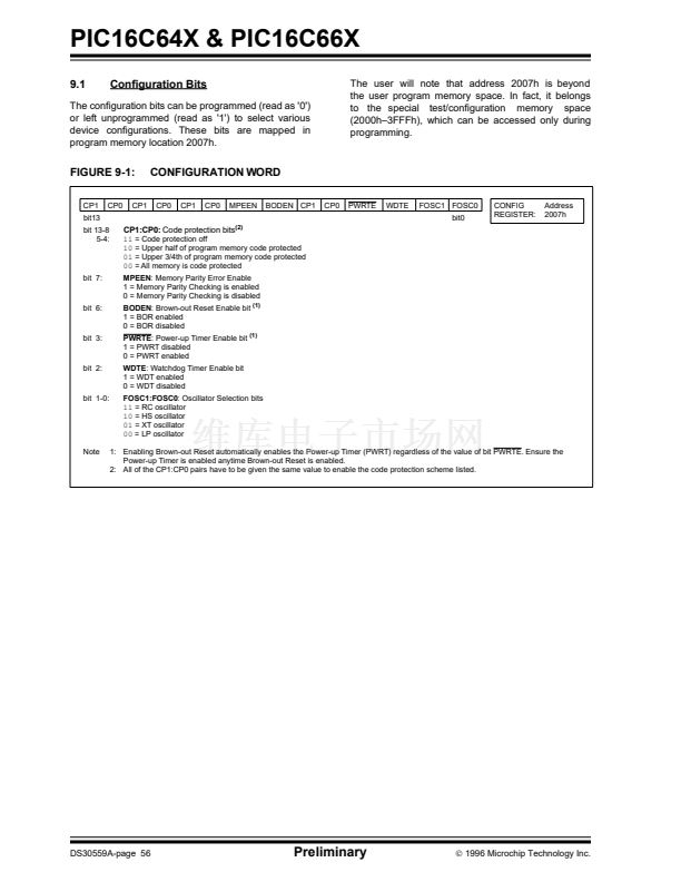
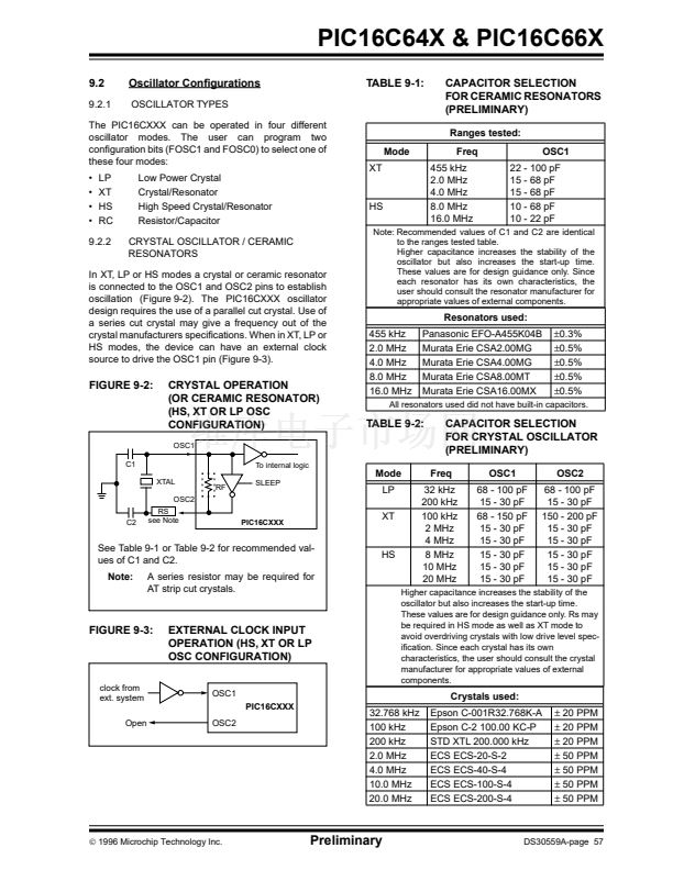
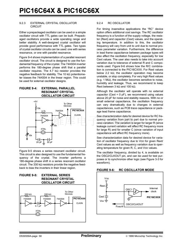
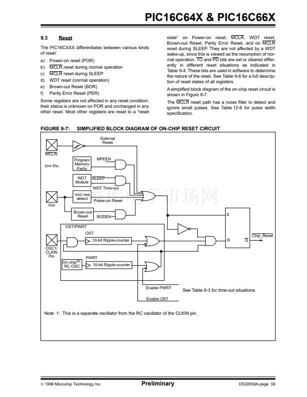
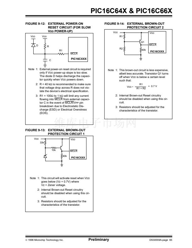
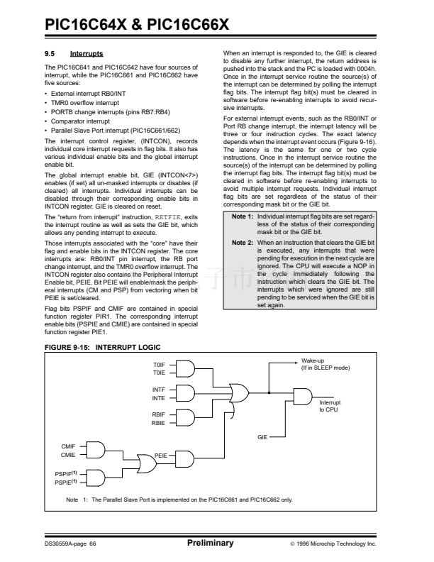
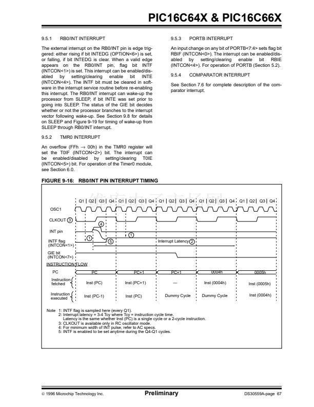
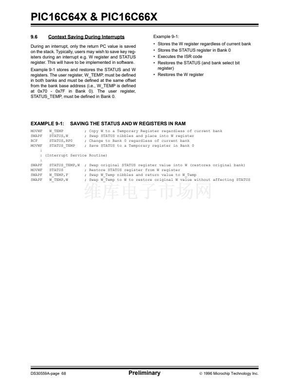
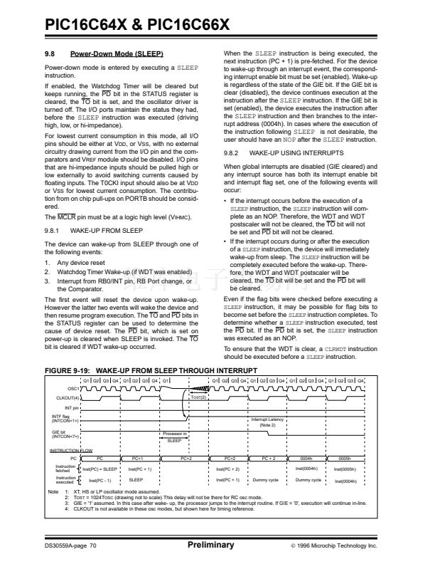
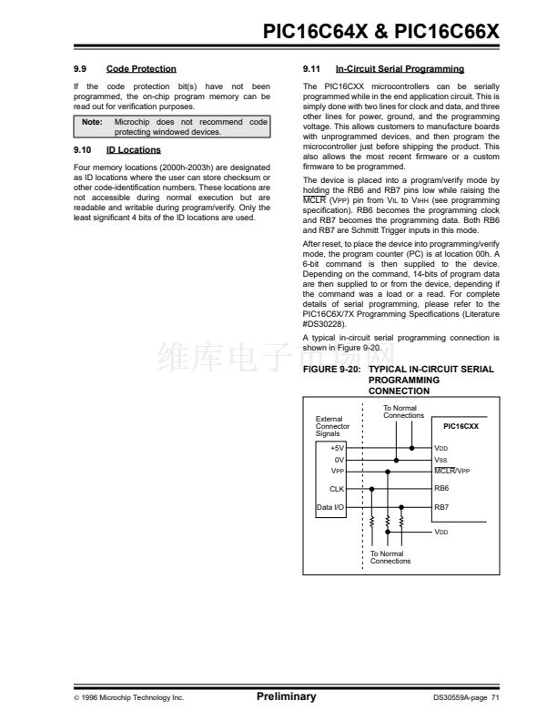
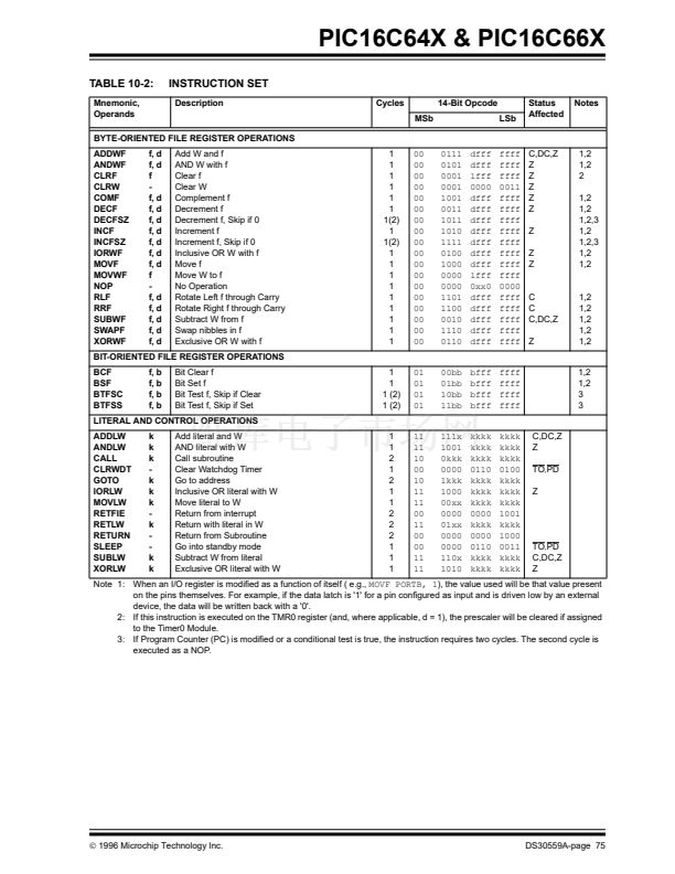
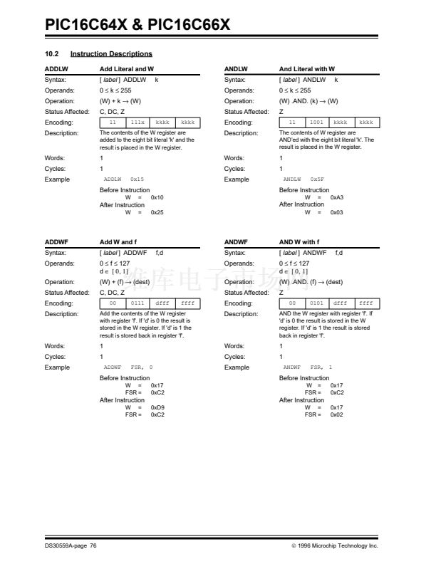
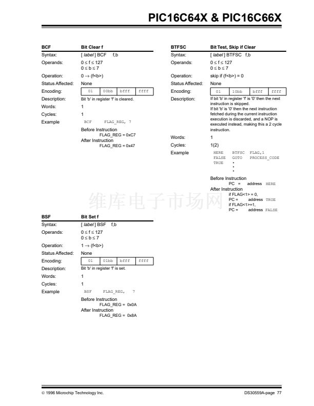
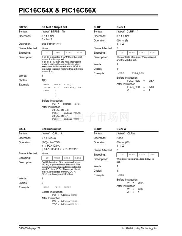
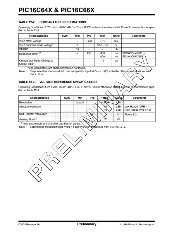
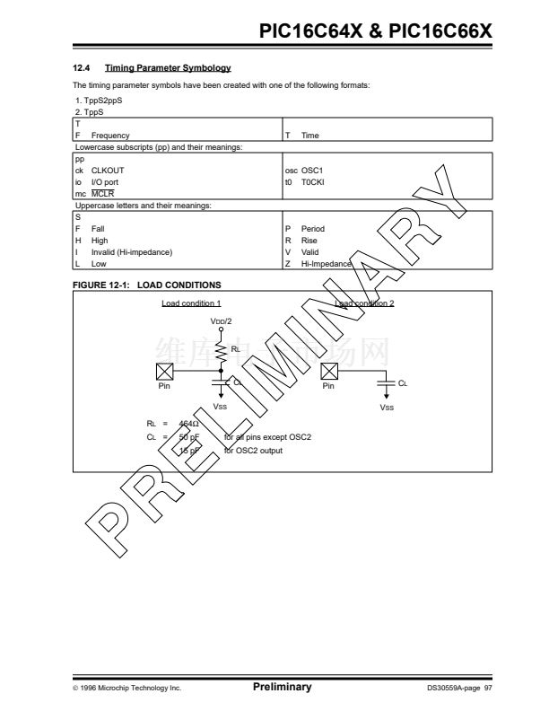
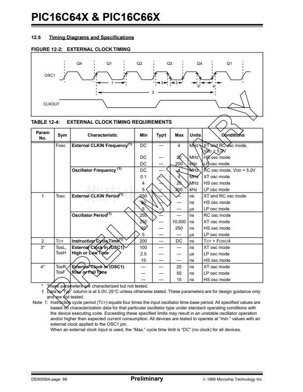
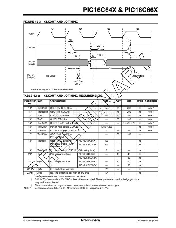
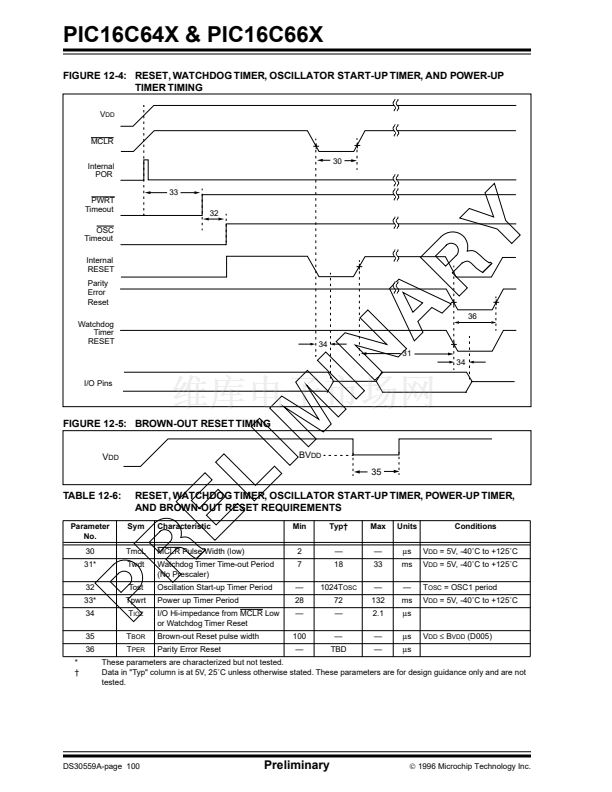
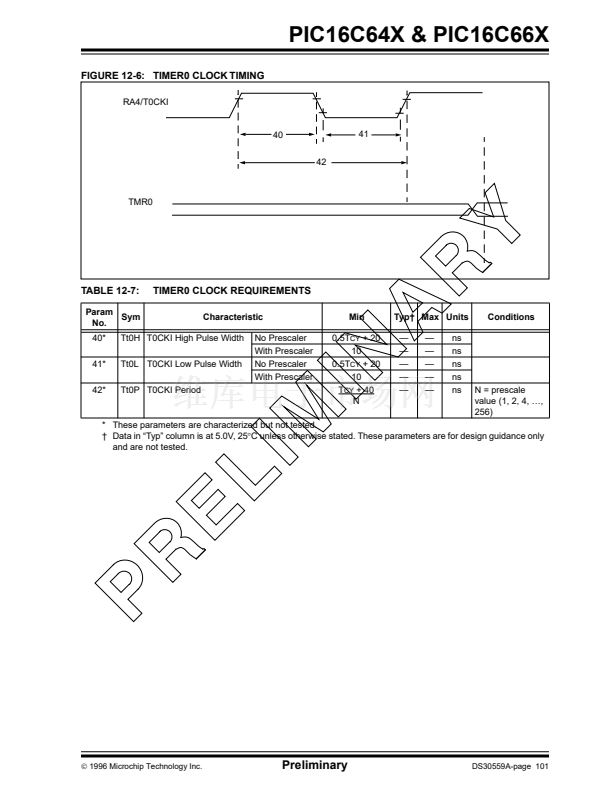
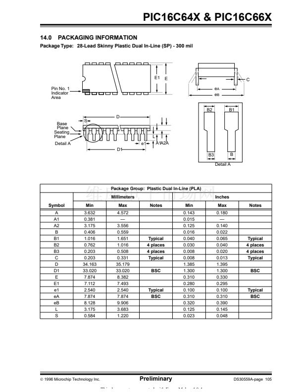
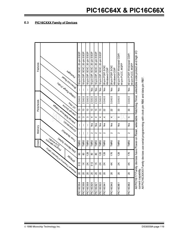
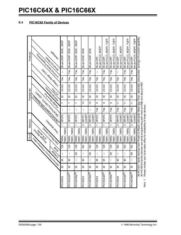
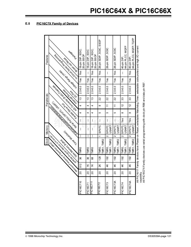
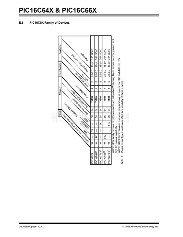
PIC16C64X & PIC16C66X
5.4
PORTD and TRISD Registers
(PIC16C661 and PIC16C662 only)
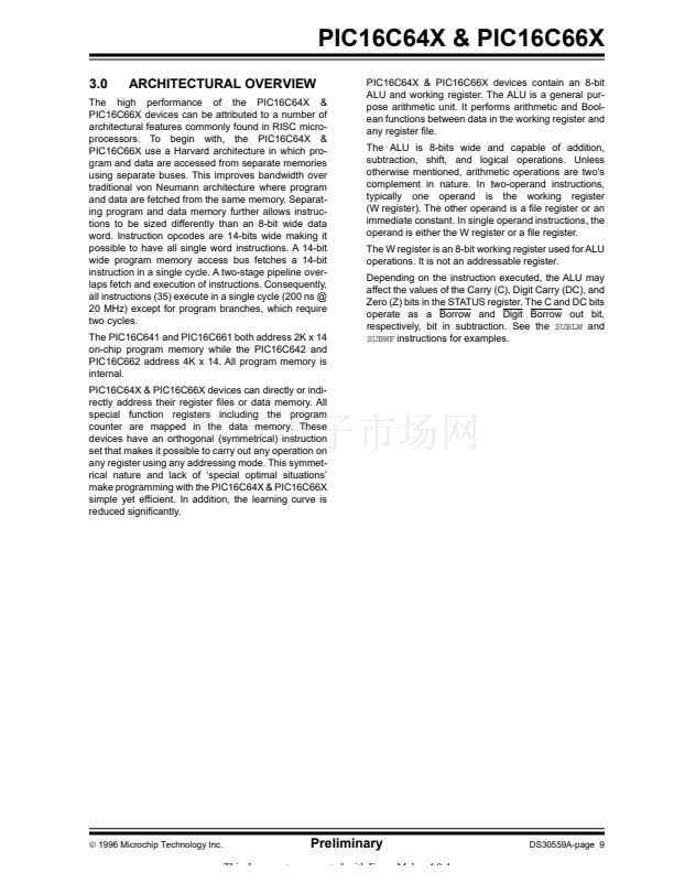
FIGURE 5-8:
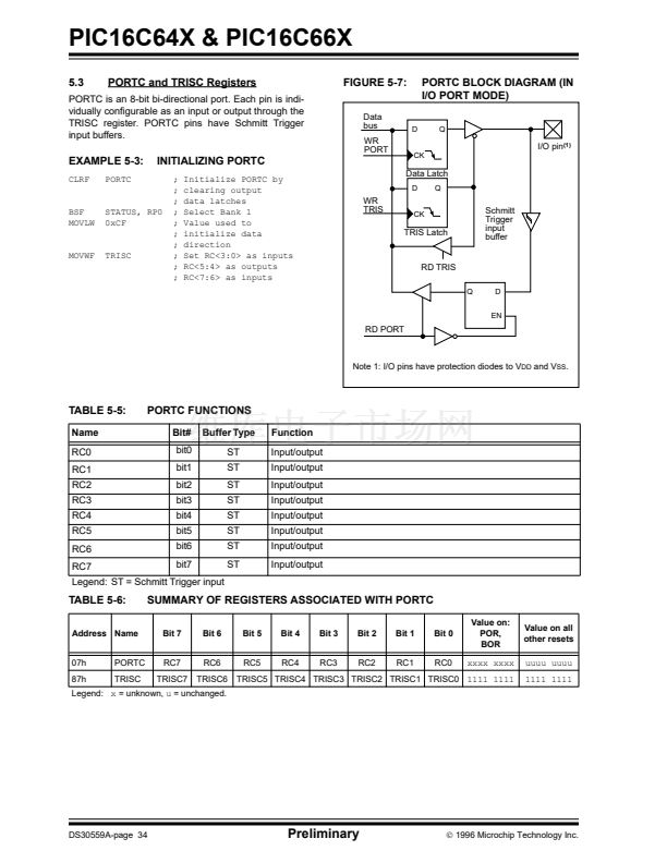
Data
bus
WR
PORT
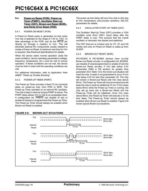
PORTD BLOCK DIAGRAM (IN
I/O PORT MODE)
D
Q
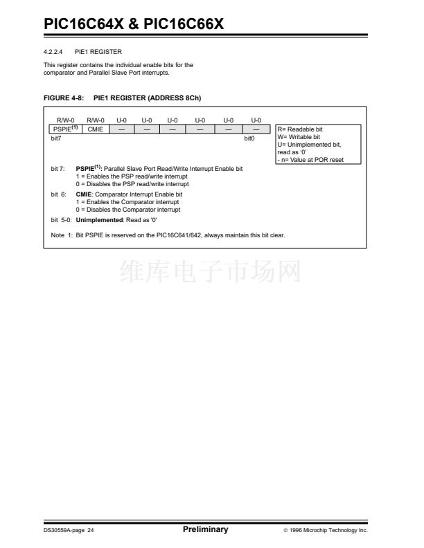
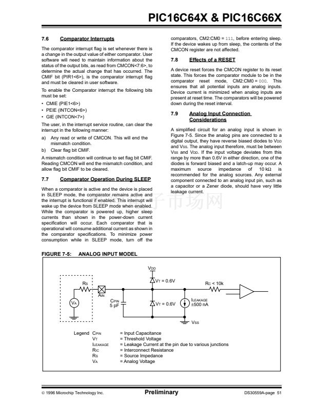
PORTD is an 8-bit port with Schmitt Trigger input buff-
ers. Each pin is individually con铿乬urable as an input or
output.
PORTD can be con铿乬ured as an 8-bit wide micropro-
cessor port (parallel slave port) by setting control bit
PSPMODE (TRISE<4>). In this mode, the input buffers
are TTL.
I/O pin
(1)
CK
Data Latch
D
Q
WR
TRIS
CK
TRIS Latch
Schmitt
Trigger
input
buffer
RD TRIS
Q
D
EN
EN
RD PORT
Note 1: I/O pins have protection diodes to V
DD
and V
SS
.
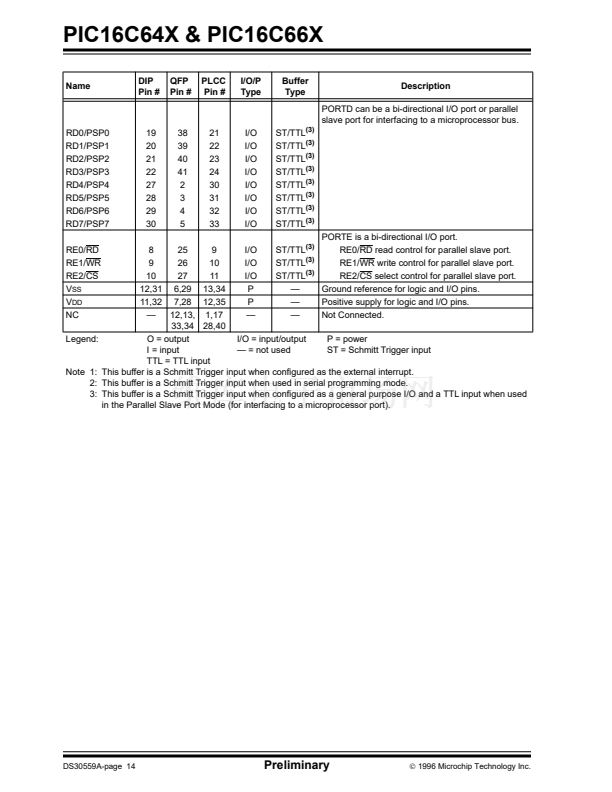
TABLE 5-7:
Name
RD0/PSP0
RD1/PSP1
RD2/PSP2
RD3/PSP3
RD4/PSP4
RD5/PSP5
RD6/PSP6
PORTD FUNCTIONS
Bit#
bit0
bit1
bit2
bit3
bit4
bit5
bit6
Buffer Type
ST/TTL
(1)
ST/TTL
(1)
ST/TTL
(1)
ST/TTL
(1)
ST/TTL
(1)
ST/TTL
(1)
ST/TTL
(1)
Function
Input/output port pin or parallel slave port bit0
Input/output port pin or parallel slave port bit1
Input/output port pin or parallel slave port bit2
Input/output port pin or parallel slave port bit3
Input/output port pin or parallel slave port bit4
Input/output port pin or parallel slave port bit5
Input/output port pin or parallel slave port bit6
RD7/PSP7
bit7
ST/TTL
(1)
Input/output port pin or parallel slave port bit7
Legend: ST = Schmitt Trigger input, TTL = TTL input
Note 1: Input buffers are Schmitt Triggers when in I/O mode and TTL buffers when in Parallel Slave Port Mode.
TABLE 5-8:
Address Name
08h
88h
89h
PORTD
TRISD
TRISE
SUMMARY OF REGISTERS ASSOCIATED WITH PORTD
Bit 7
RD7
Bit 6
RD6
Bit 5
RD5
Bit 4
RD4
TRISD4
PSPMODE
Bit 3
RD3
Bit 2
RD2
Bit 1
RD1
Bit 0
RD0
Value on:
POR,
BOR
xxxx xxxx
Value on all
other resets
uuuu uuuu
1111 1111
0000 -111
TRISD7 TRISD6 TRISD5
IBF
OBF
IBOV
TRISD3 TRISD2 TRISD1 TRISD0
1111 1111
鈥?/div>
TRISE2 TRISE1 TRISE0
0000 -111
Legend:
x
= unknown,
u
= unchanged,
-
= unimplemented read as '0'. Shaded cells are not used by PORTD.
漏
1996 Microchip Technology Inc.
Preliminary
DS30559A-page 35


 1
1
 2
2
 3
3
 4
4
 5
5
 6
6
 7
7
 8
8
 9
9
 10
10
 11
11
 12
12
 13
13
 14
14
 15
15
 16
16
 17
17
 18
18
 19
19
 20
20
 21
21
 22
22
 23
23
 24
24
 25
25
 26
26
 27
27
 28
28
 29
29
 30
30
 31
31
 32
32
 33
33
 34
34
 35
35
 36
36
 37
37
 38
38
 39
39
 40
40
 41
41
 42
42
 43
43
 44
44
 45
45
 46
46
 47
47
 48
48
 49
49
 50
50
 51
51
 52
52
 53
53
 54
54
 55
55
 56
56
 57
57
 58
58
 59
59
 60
60
 61
61
 62
62
 63
63
 64
64
 65
65
 66
66
 67
67
 68
68
 69
69
 70
70
 71
71
 72
72
 73
73
 74
74
 75
75
 76
76
 77
77
 78
78
 79
79
 80
80
 81
81
 82
82
 83
83
 84
84
 85
85
 86
86
 87
87
 88
88
 89
89
 90
90
 91
91
 92
92
 93
93
 94
94
 95
95
 96
96
 97
97
 98
98
 99
99
 100
100
 101
101
 102
102
 103
103
 104
104
 105
105
 106
106
 107
107
 108
108
 109
109
 110
110
 111
111
 112
112
 113
113
 114
114
 115
115
 116
116
 117
117
 118
118
 119
119
 120
120
 121
121
 122
122
 123
123
 124
124
 125
125
 126
126
 127
127
 128
128
 129
129
 130
130
 131
131
 132
132
 133
133
 134
134
 135
135
 136
136
