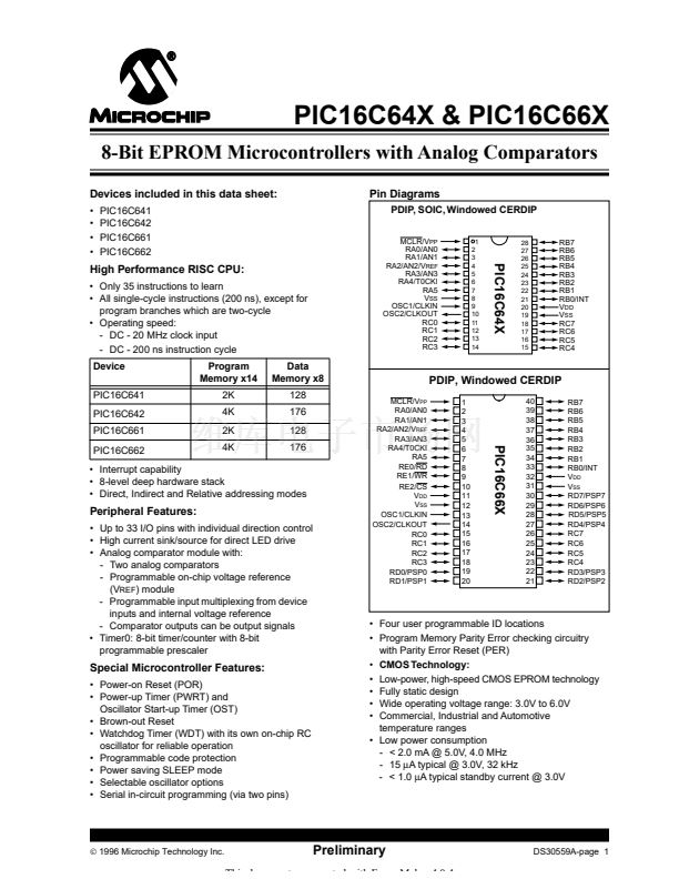
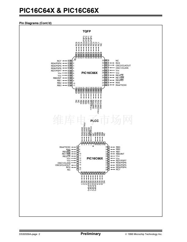
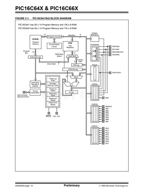
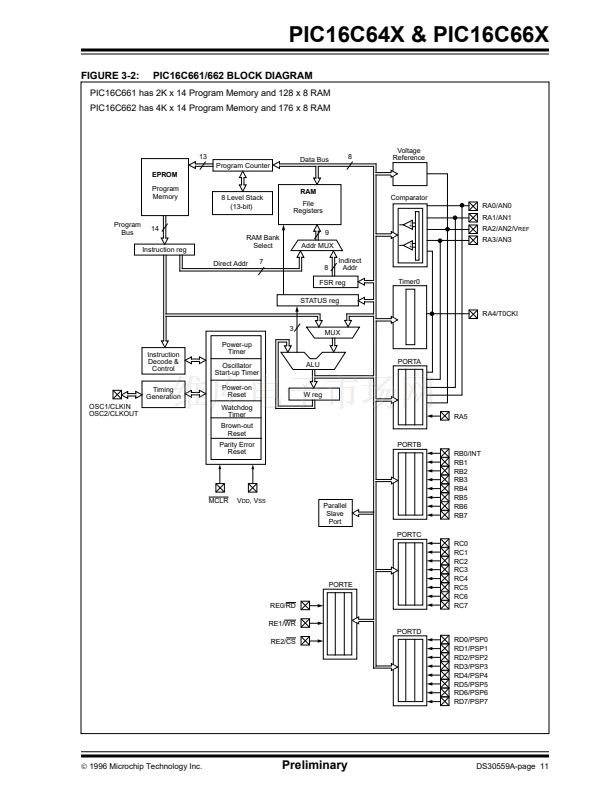
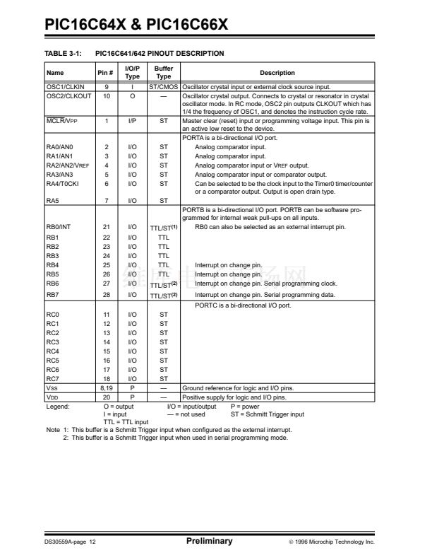
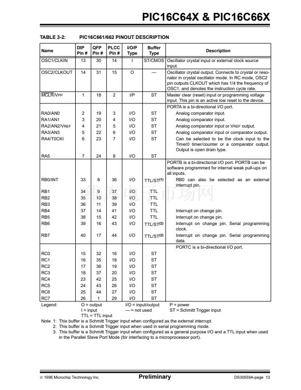
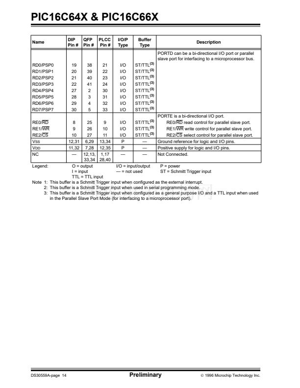
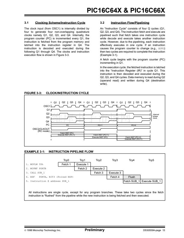
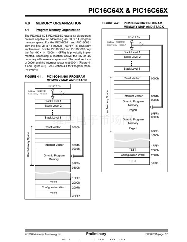
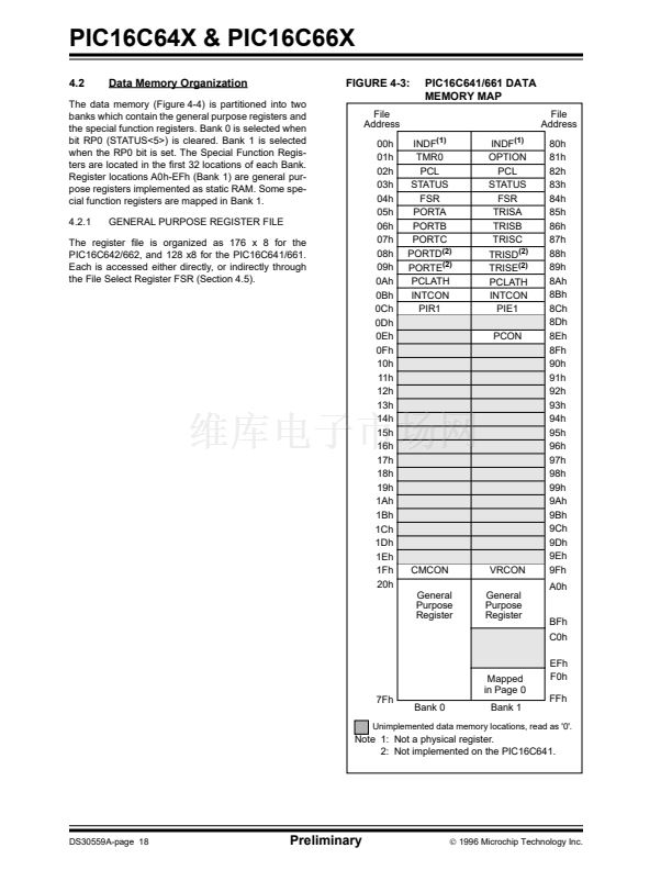
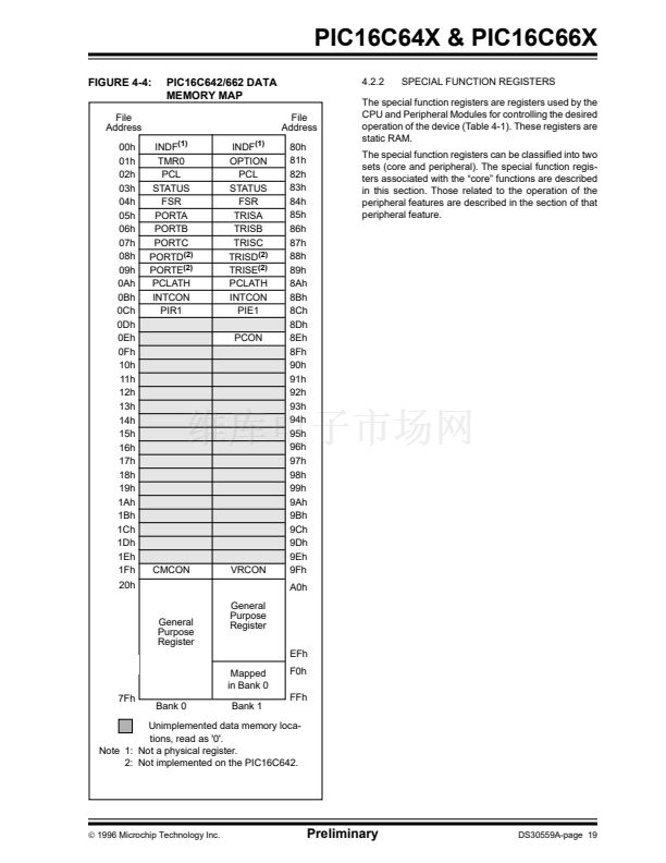
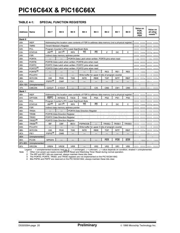
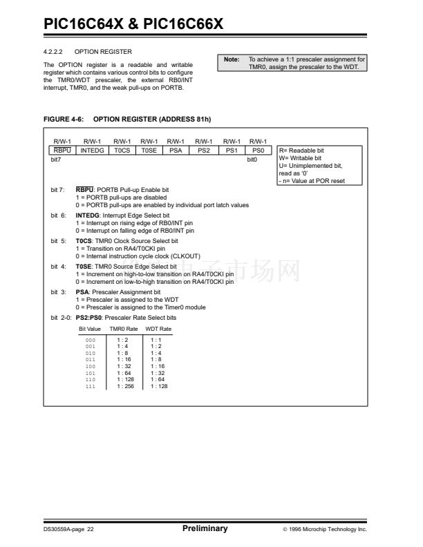
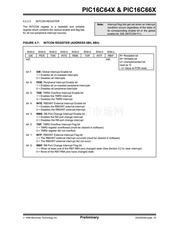
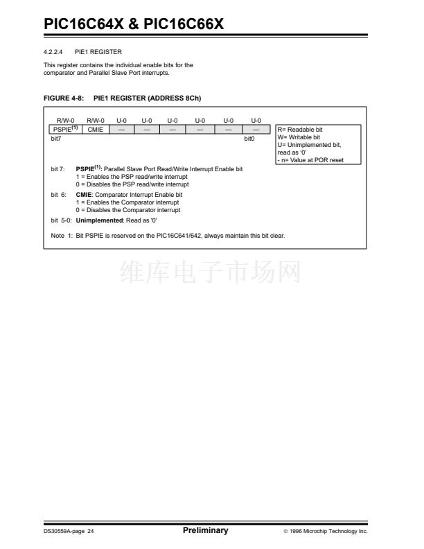
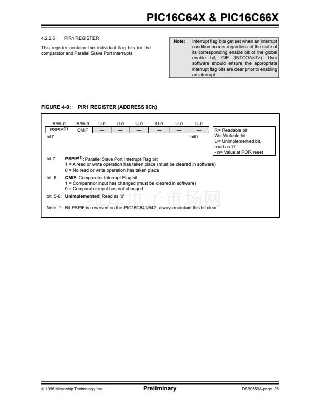
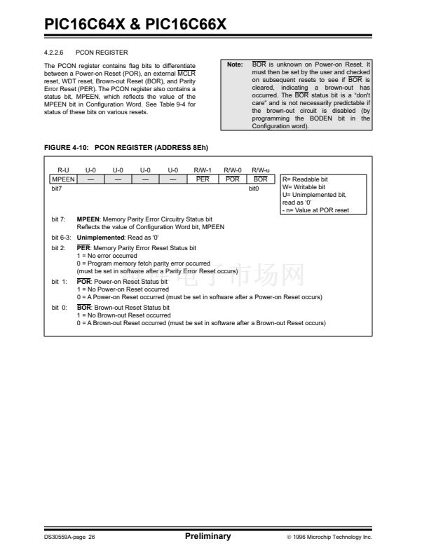
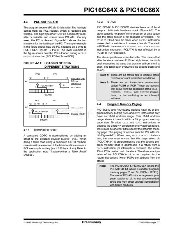
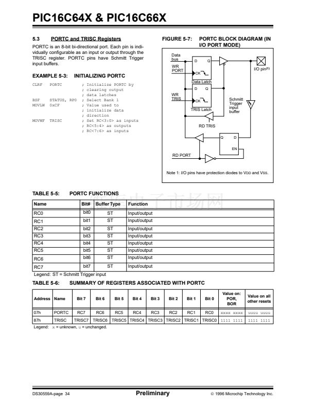
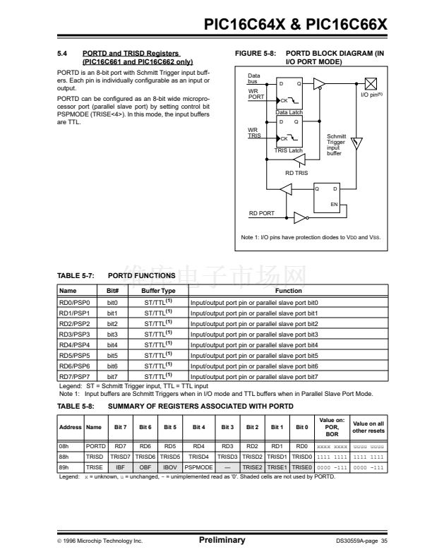
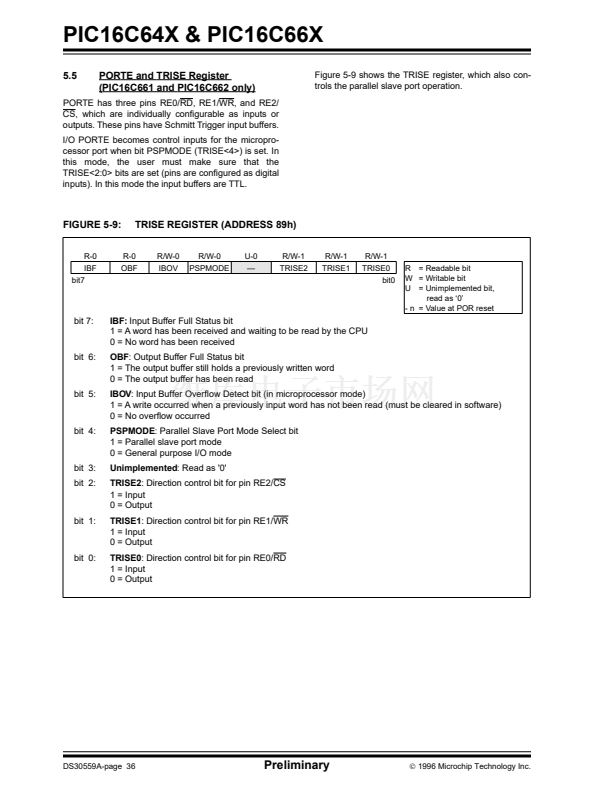
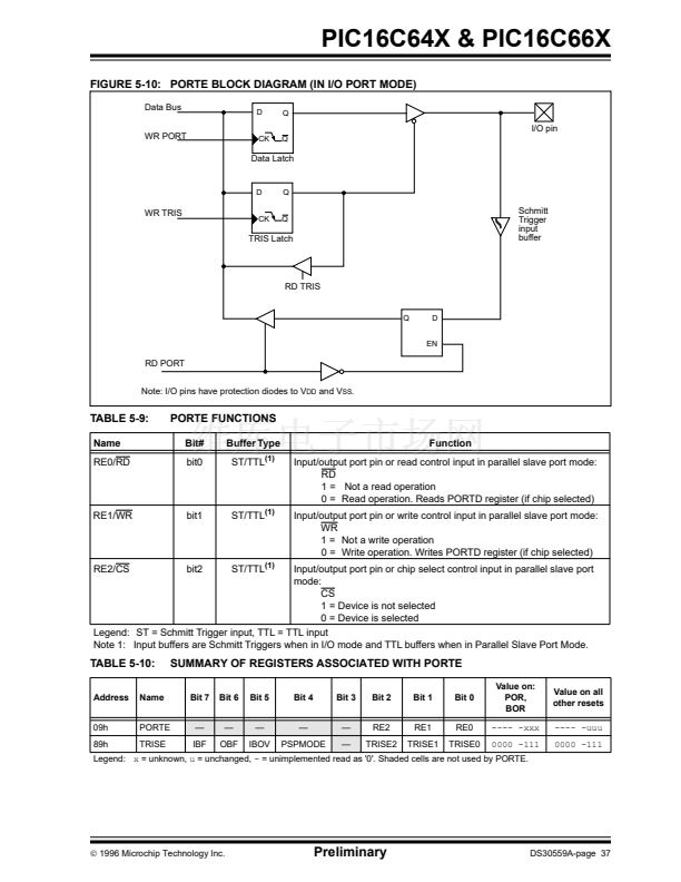
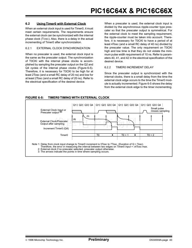
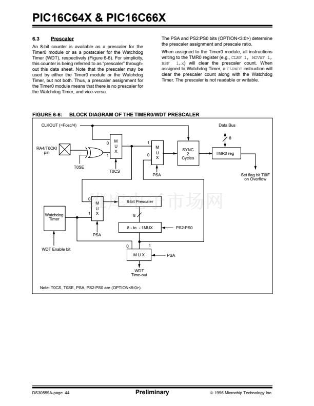
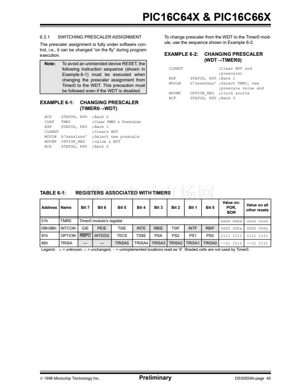
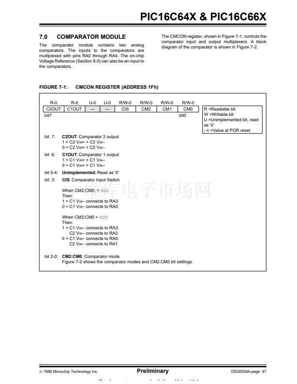
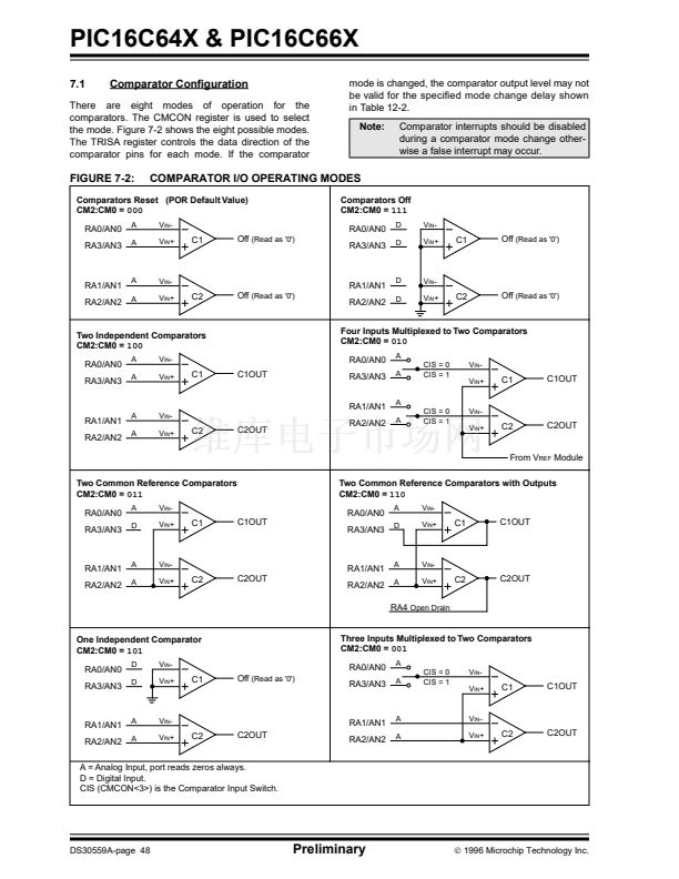
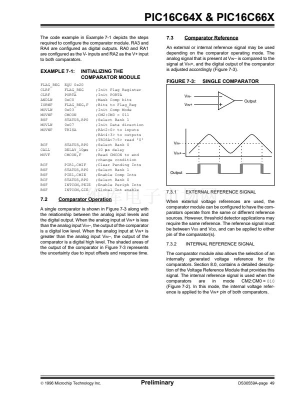
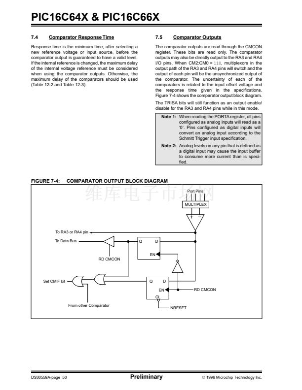
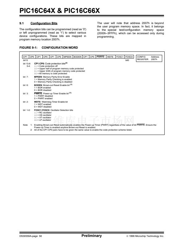
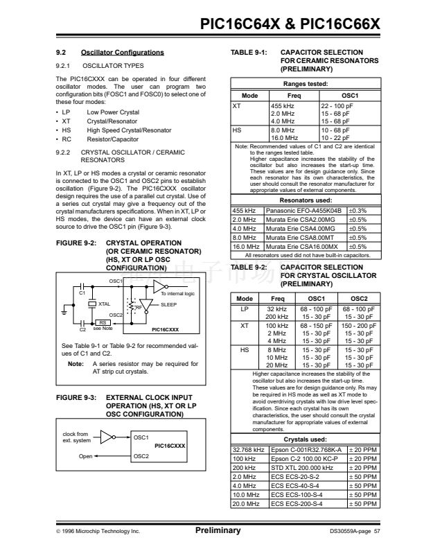
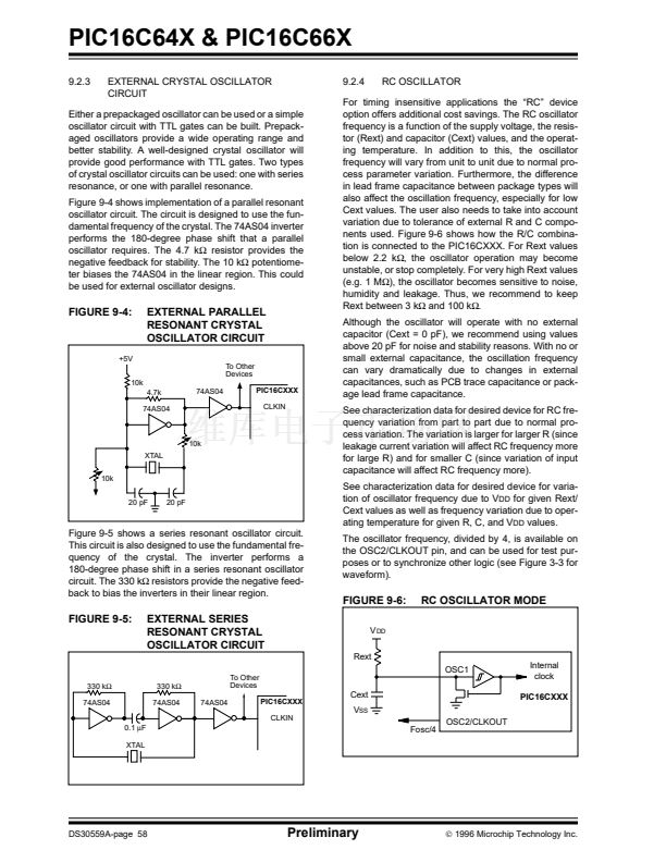
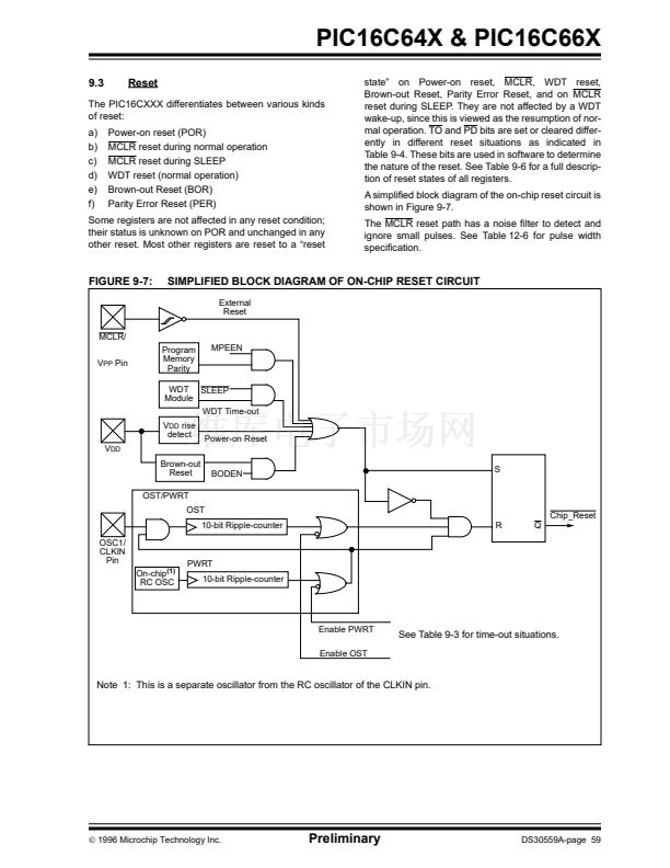
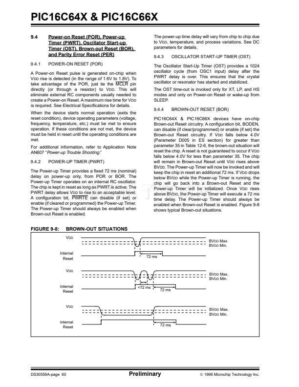
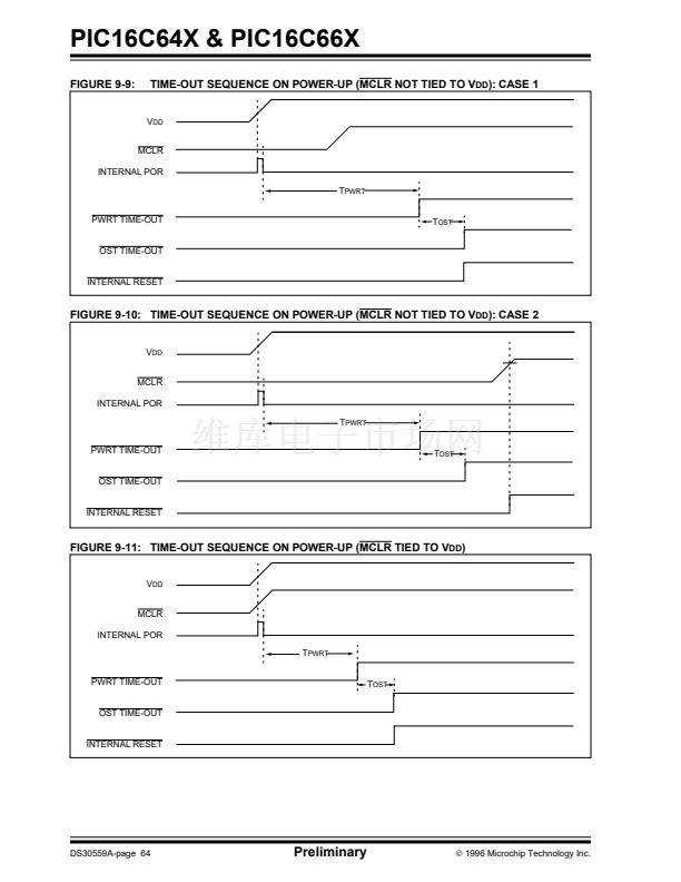
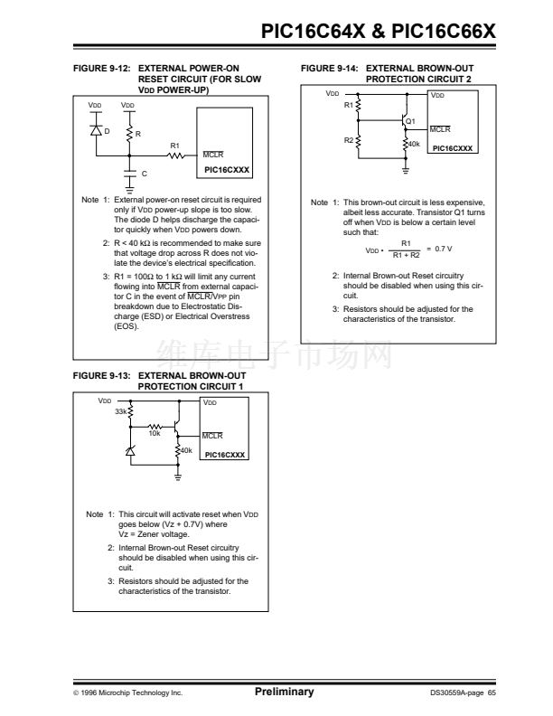
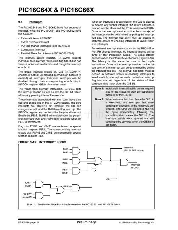
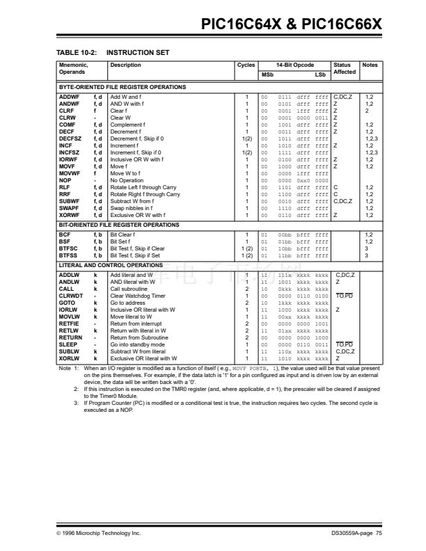
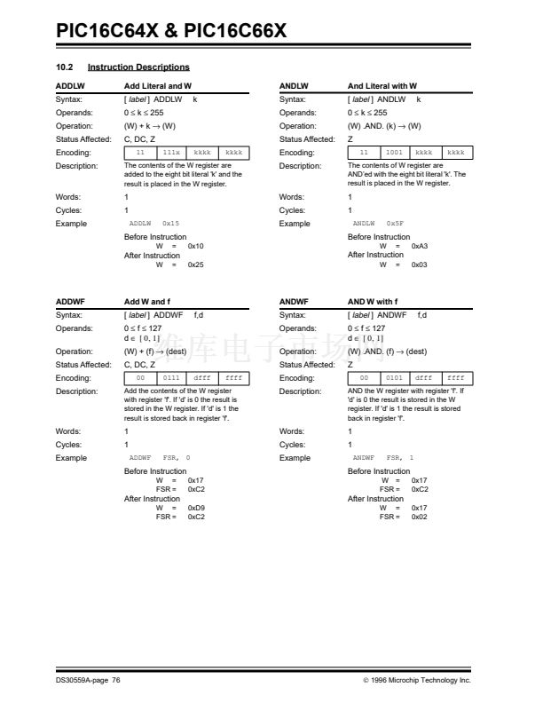
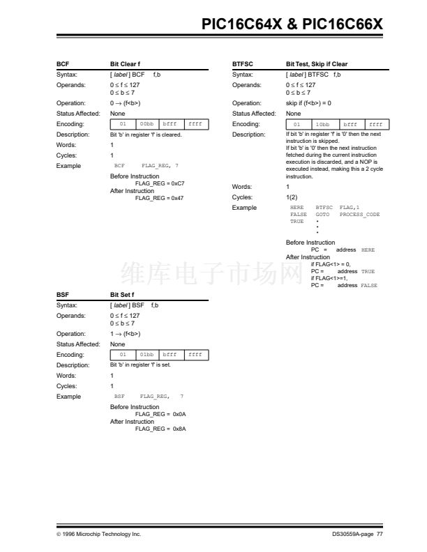
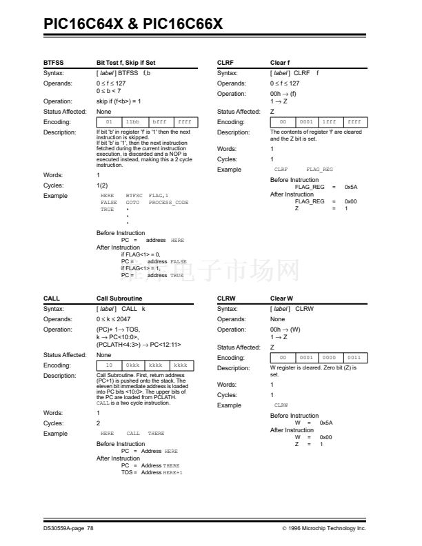
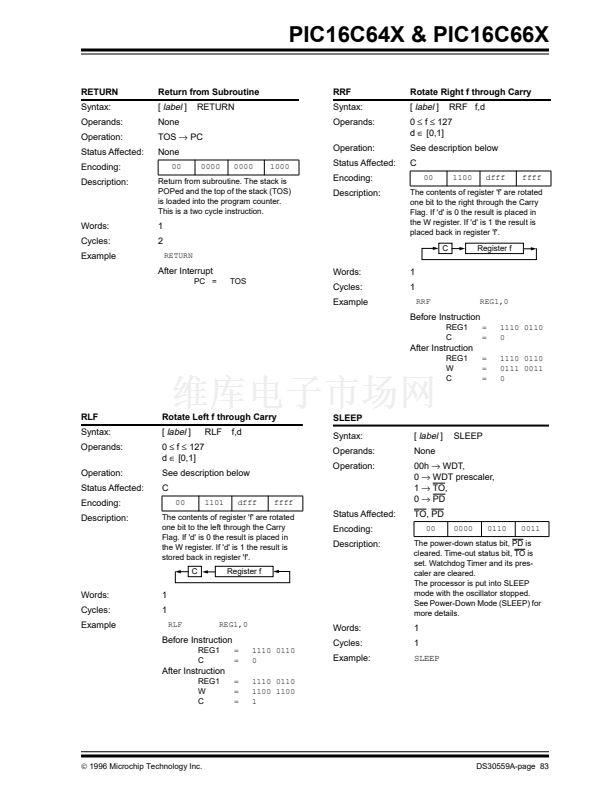
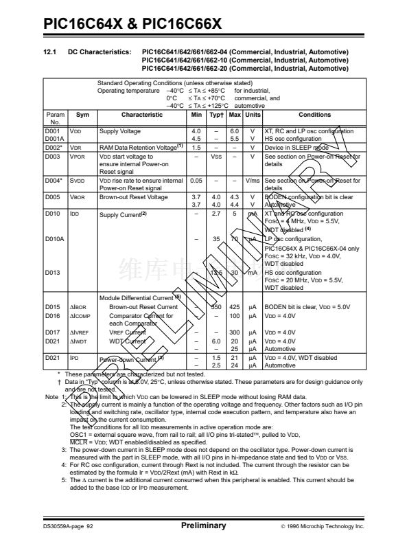
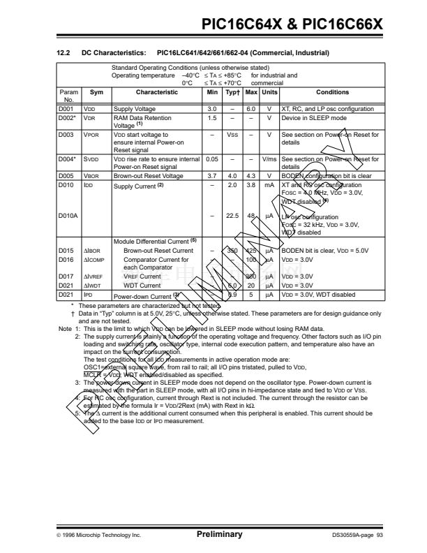
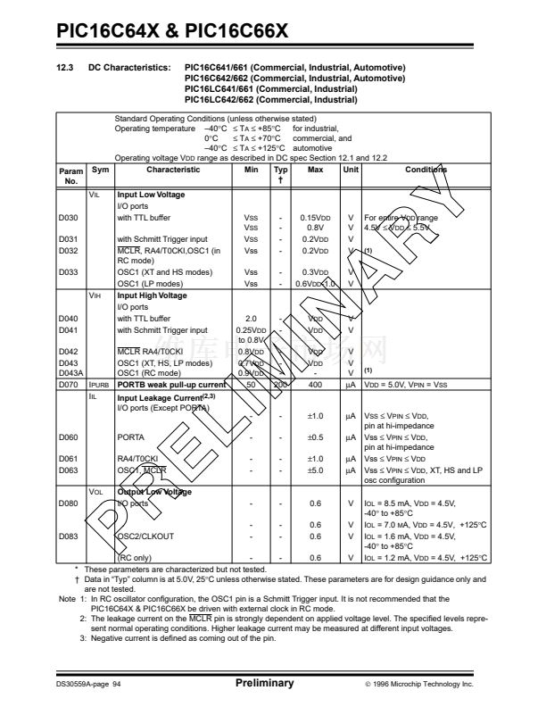
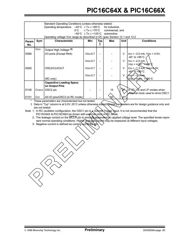
PIC16C64X & PIC16C66X
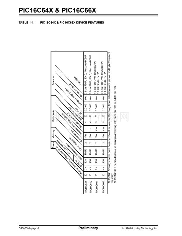
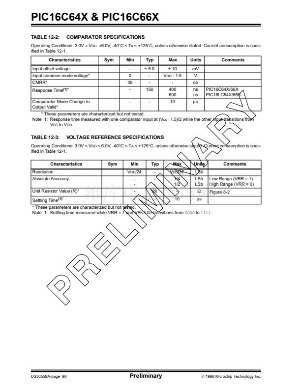
TABLE 12-2:
COMPARATOR SPECIFICATIONS
Operating Conditions: 3.0V
<
V
DD
<
6.0V, -40藲C < T
A
< +125藲C, unless otherwise stated. Current consumption is spec-
i铿乪d in Table 12-1.
Characteristics
Input offset voltage
Input common mode voltage*
CMRR*
Response Time
(1)*
Comparator Mode Change to
Output Valid*
Sym
Min
-
0
35
-
-
Typ
卤
5.0
-
-
150
-
Max
卤
10
V
DD
- 1.5
-
400
600
10
Units
mV
V
db
ns
ns
碌s
PIC16C64X/66X
PIC16LC64X/66X
Comments
* These parameters are characterized but not tested.
Note 1: Response time measured with one comparator input at (V
DD
-
1.5)/2 while the other input transitions from
V
SS
to V
DD
.
TABLE 12-3:
VOLTAGE REFERENCE SPECIFICATIONS
Operating Conditions: 3.0V < V
DD
< 6.0V, -40掳C < T
A
< +125掳C, unless otherwise stated. Current consumption is spec-
i铿乪d in Table 12-1.
Characteristics
Resolution
Absolute Accuracy
Unit Resistor Value (R)*
Settling Time
(1)*
Sym
Min
V
DD
/24
-
-
-
-
Typ
-
-
-
2k
-
Max
V
DD
/32
1/4
1/2
-
10
Units
LSb
LSb
LSb
鈩?/div>
碌s
Low Range (VRR = 1)
High Range (VRR = 0)
Figure 8-2
Comments
* These parameters are characterized but not tested.
Note 1: Settling time measured while VRR = 1 and VR<3:0> transitions from
0000
to
1111.
DS30559A-page 96
Preliminary
漏
1996 Microchip Technology Inc.


 1
1
 2
2
 3
3
 4
4
 5
5
 6
6
 7
7
 8
8
 9
9
 10
10
 11
11
 12
12
 13
13
 14
14
 15
15
 16
16
 17
17
 18
18
 19
19
 20
20
 21
21
 22
22
 23
23
 24
24
 25
25
 26
26
 27
27
 28
28
 29
29
 30
30
 31
31
 32
32
 33
33
 34
34
 35
35
 36
36
 37
37
 38
38
 39
39
 40
40
 41
41
 42
42
 43
43
 44
44
 45
45
 46
46
 47
47
 48
48
 49
49
 50
50
 51
51
 52
52
 53
53
 54
54
 55
55
 56
56
 57
57
 58
58
 59
59
 60
60
 61
61
 62
62
 63
63
 64
64
 65
65
 66
66
 67
67
 68
68
 69
69
 70
70
 71
71
 72
72
 73
73
 74
74
 75
75
 76
76
 77
77
 78
78
 79
79
 80
80
 81
81
 82
82
 83
83
 84
84
 85
85
 86
86
 87
87
 88
88
 89
89
 90
90
 91
91
 92
92
 93
93
 94
94
 95
95
 96
96
 97
97
 98
98
 99
99
 100
100
 101
101
 102
102
 103
103
 104
104
 105
105
 106
106
 107
107
 108
108
 109
109
 110
110
 111
111
 112
112
 113
113
 114
114
 115
115
 116
116
 117
117
 118
118
 119
119
 120
120
 121
121
 122
122
 123
123
 124
124
 125
125
 126
126
 127
127
 128
128
 129
129
 130
130
 131
131
 132
132
 133
133
 134
134
 135
135
 136
136
