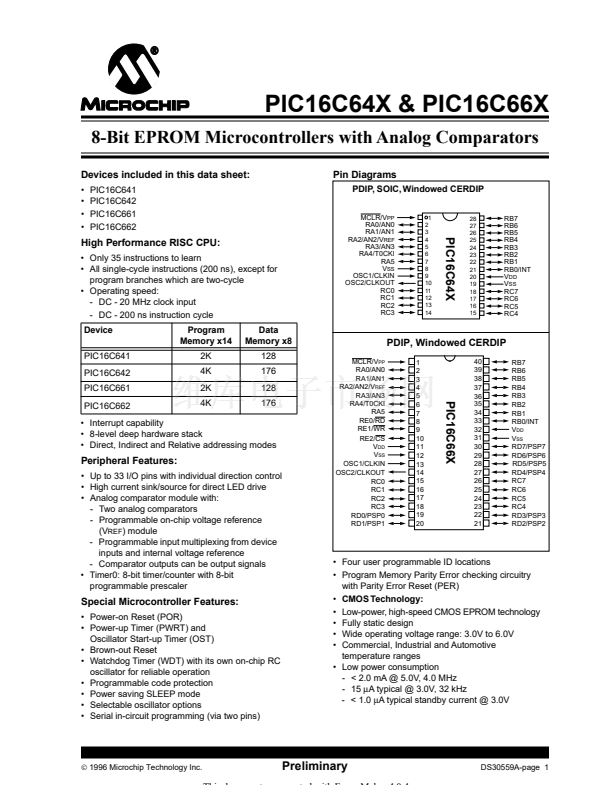
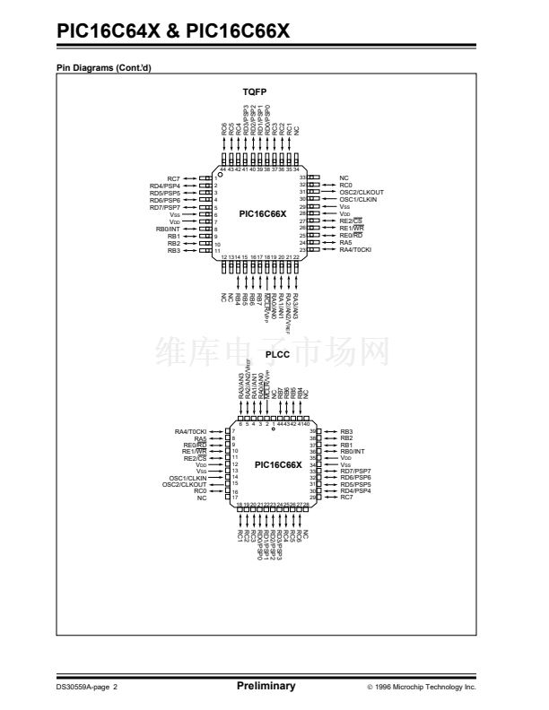
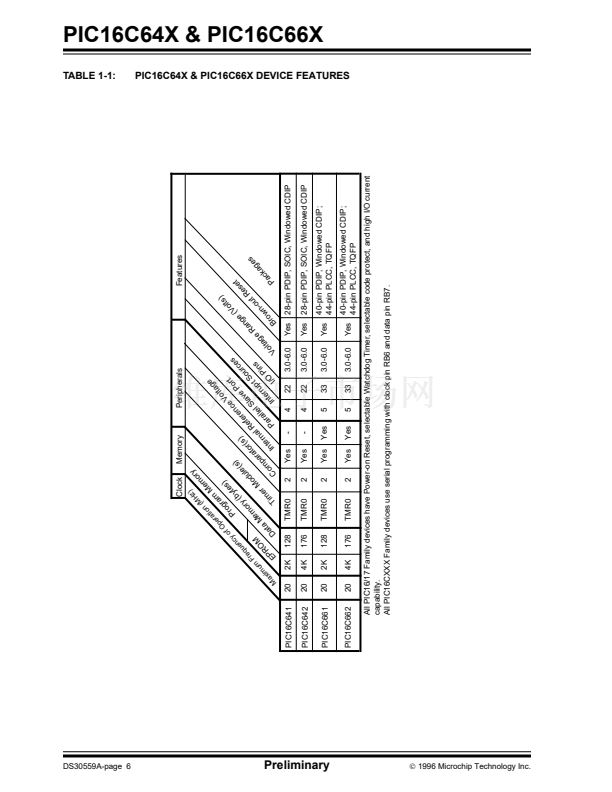
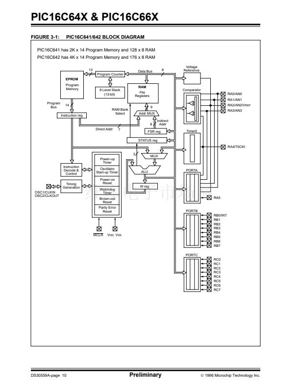
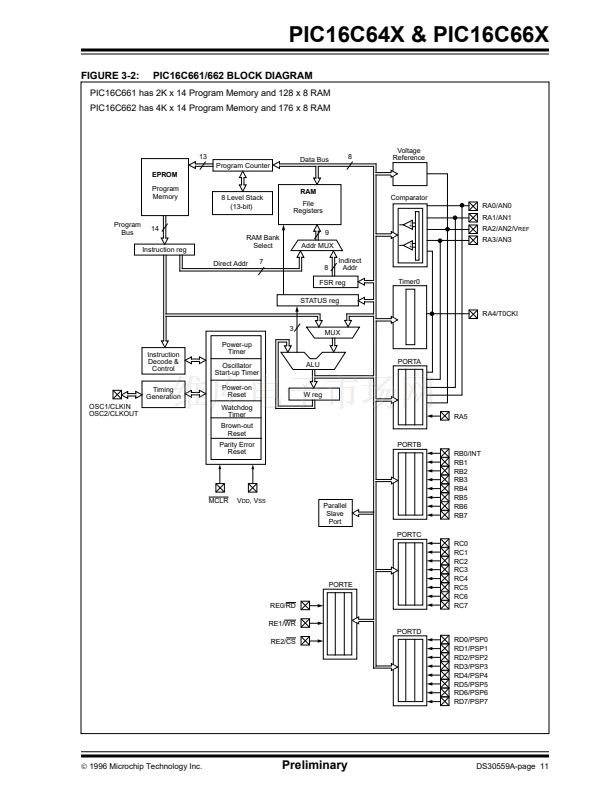
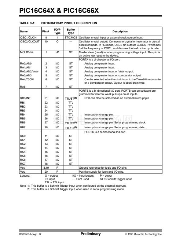
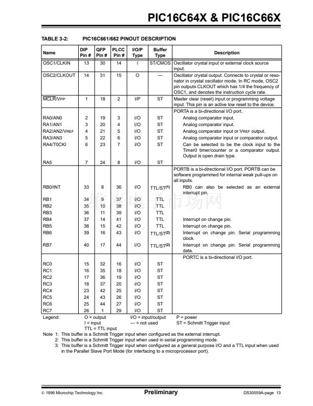
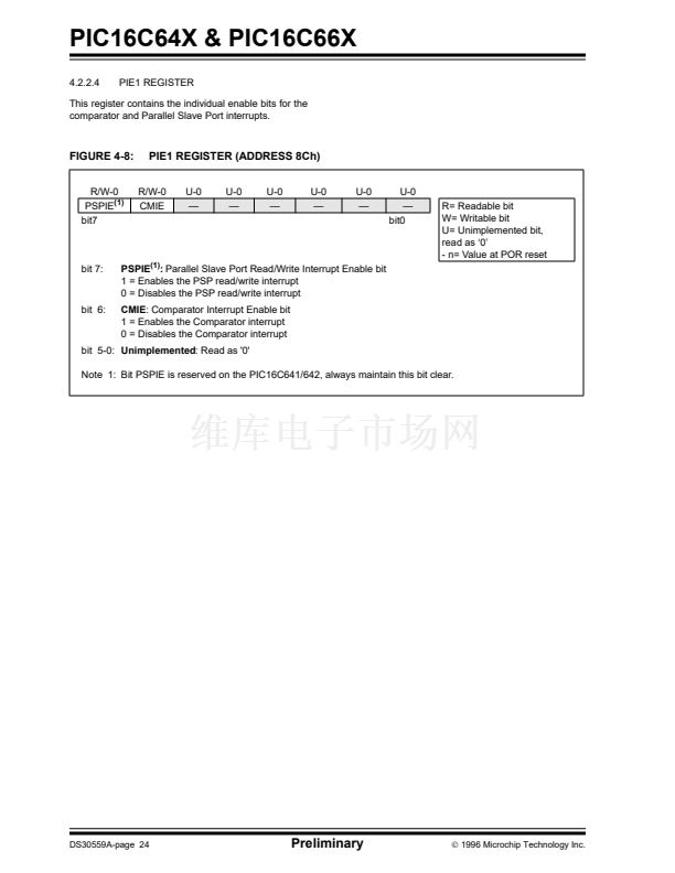
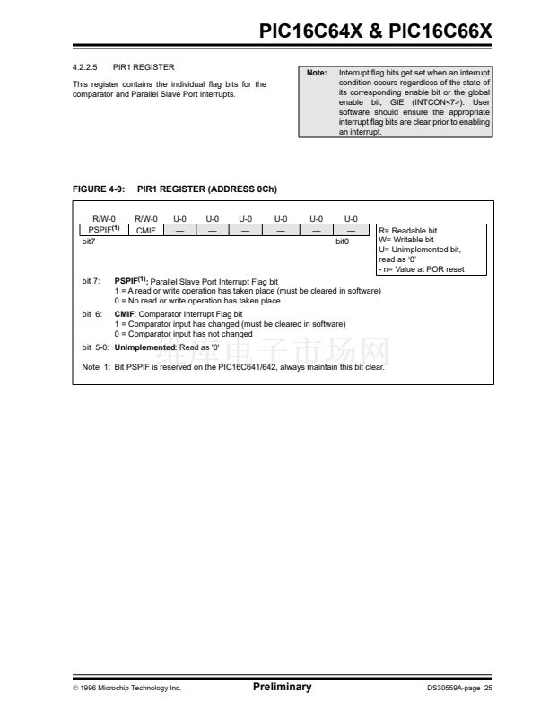
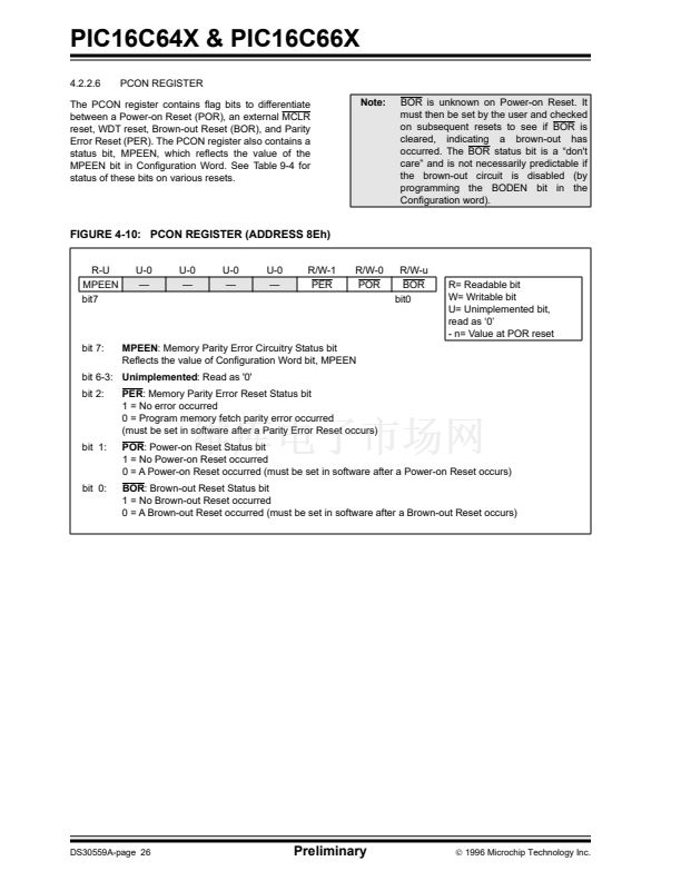
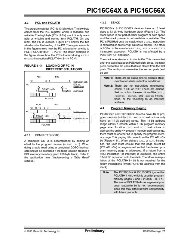
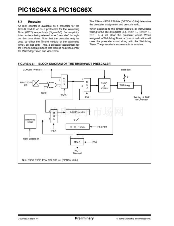
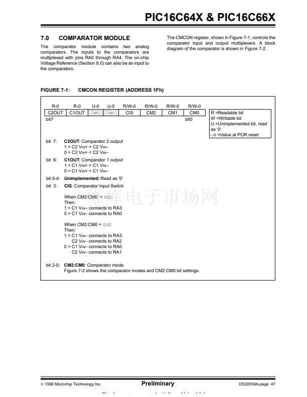
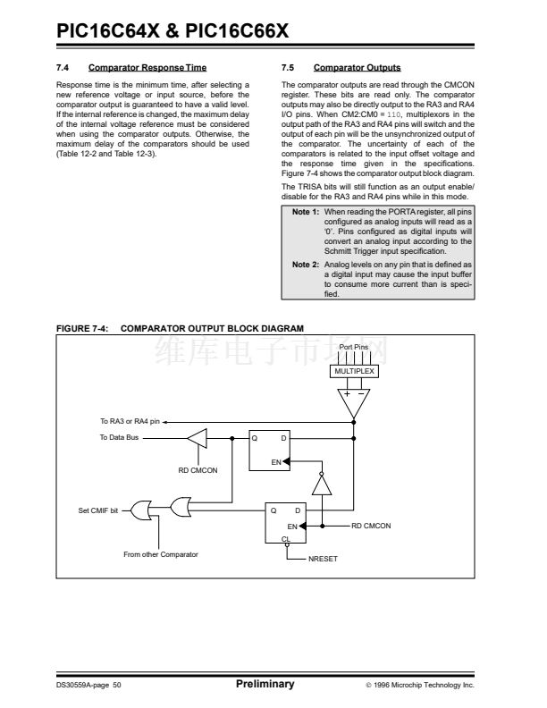
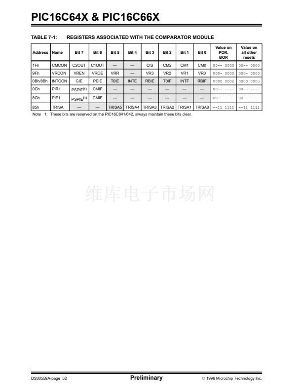
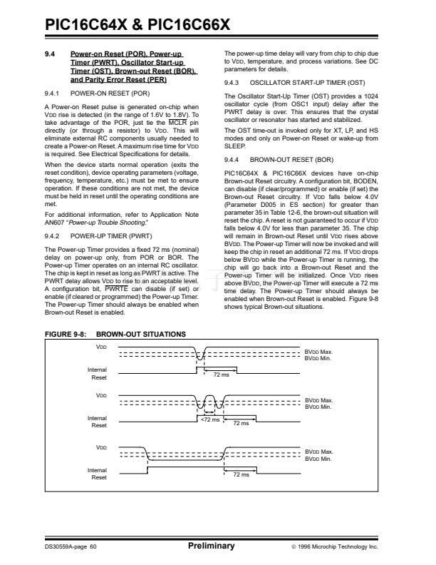
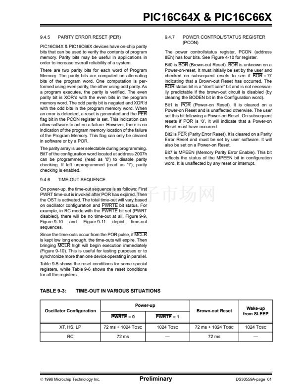
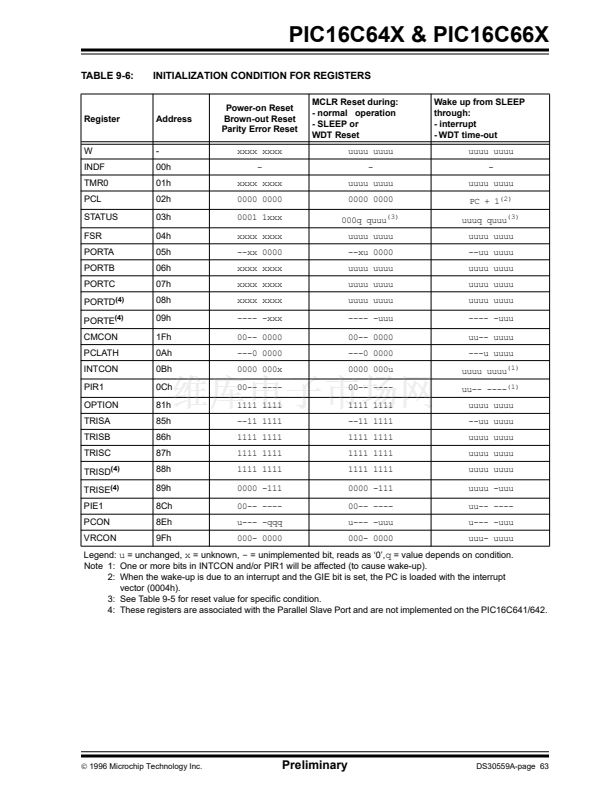
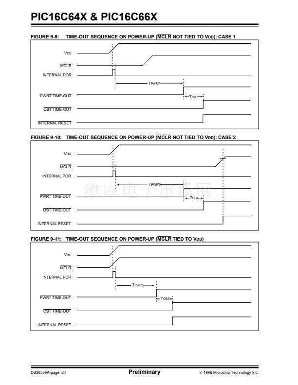
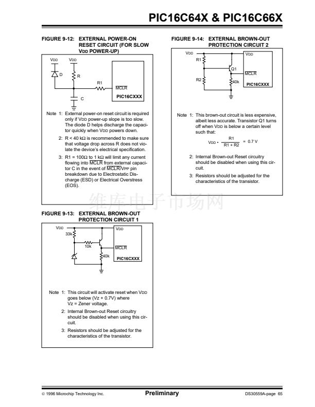
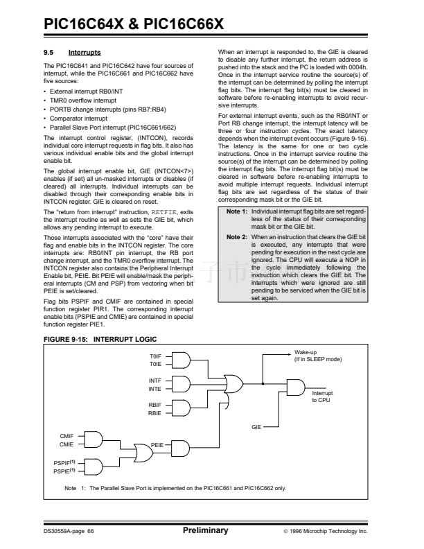
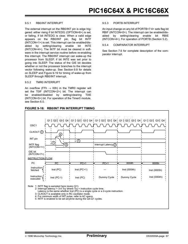
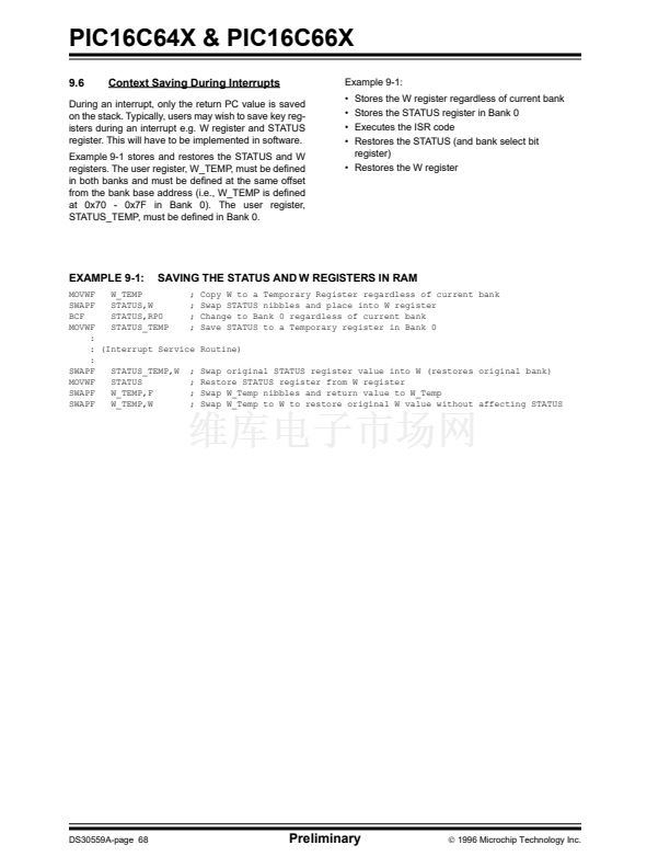
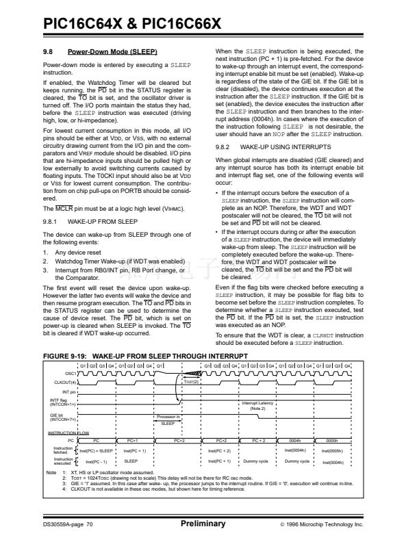
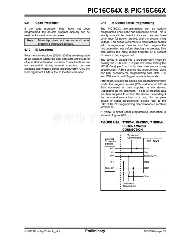
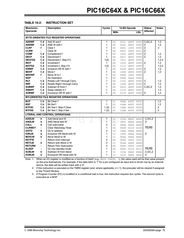
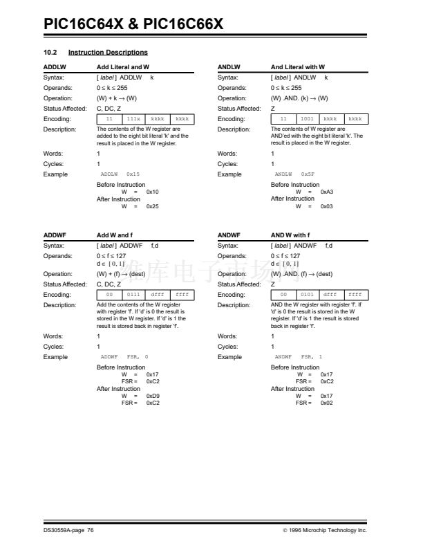
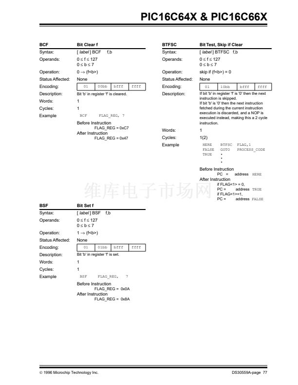
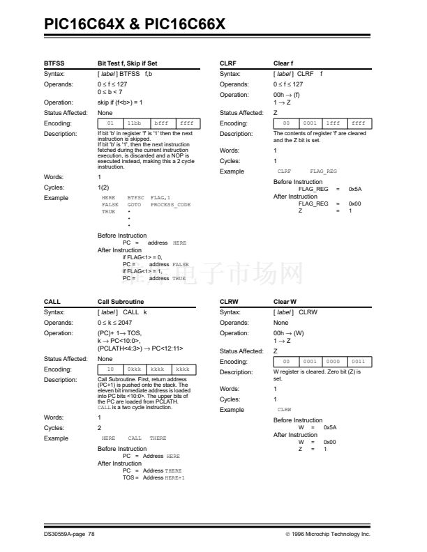
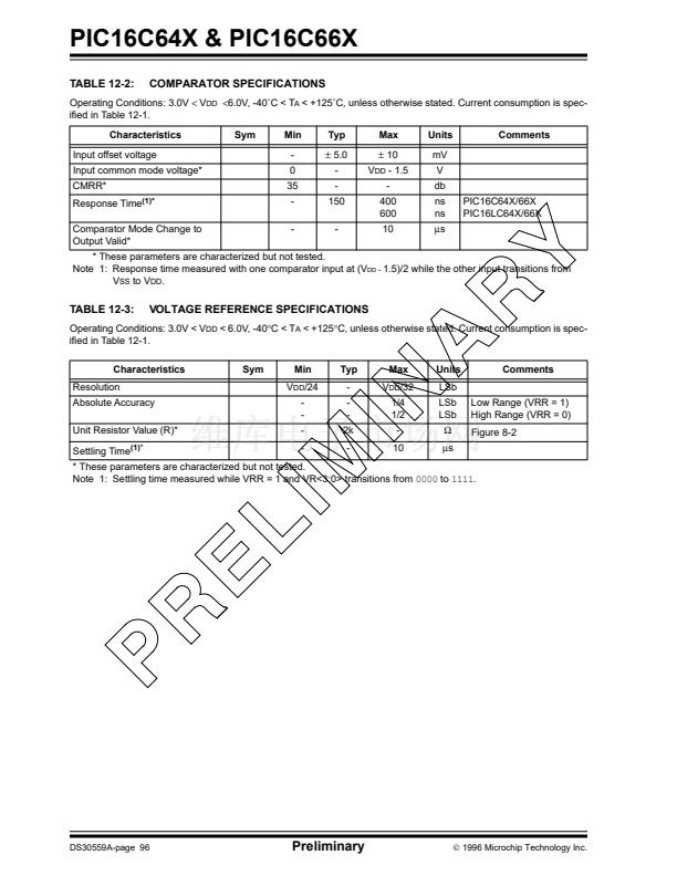
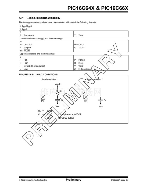
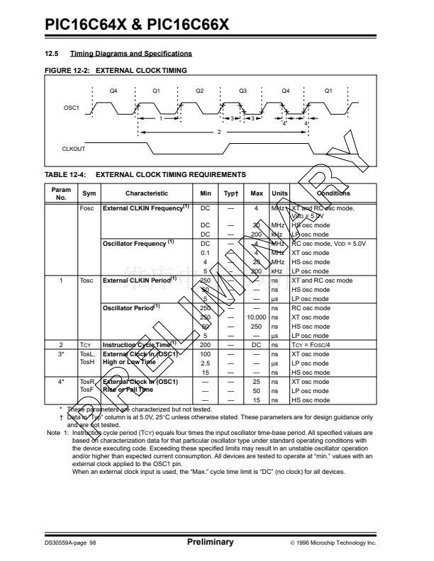
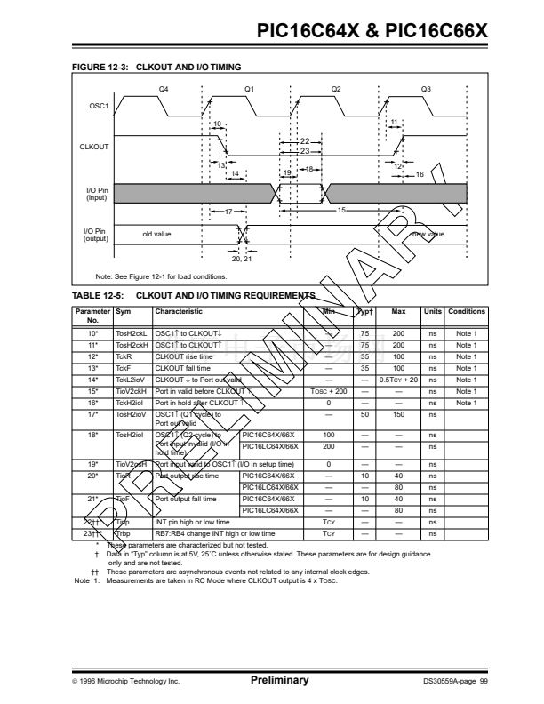
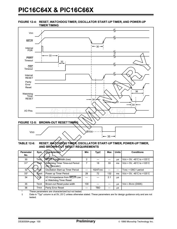
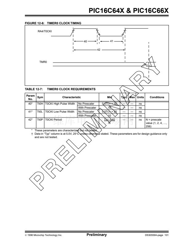
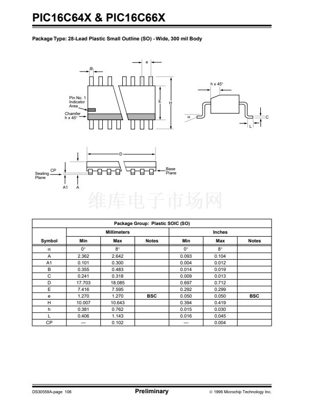
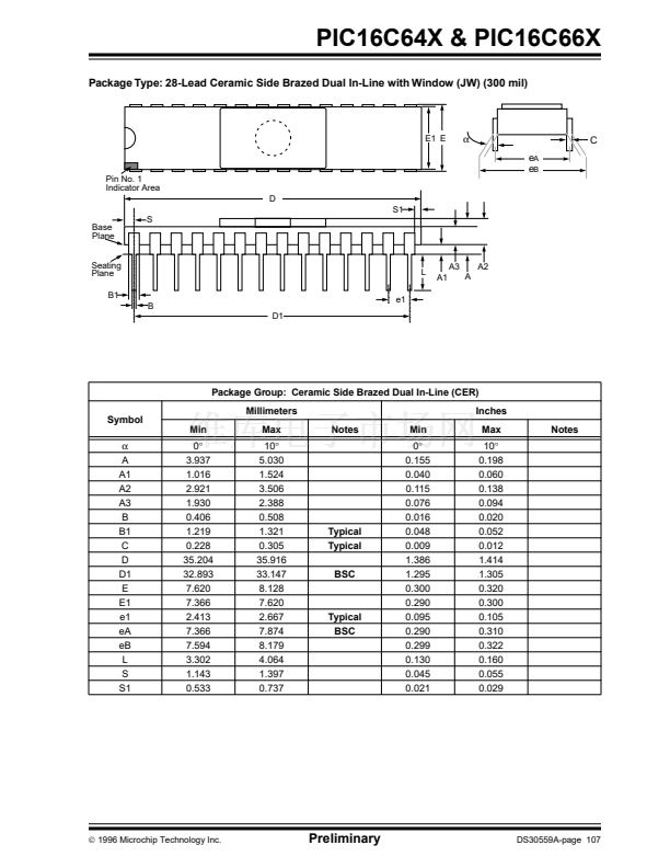
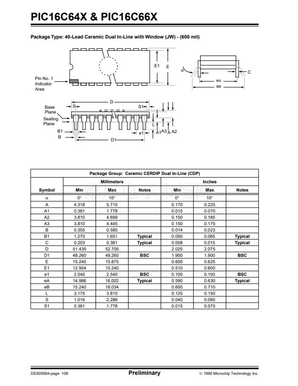
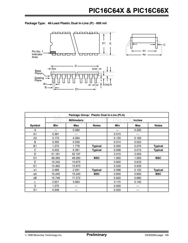
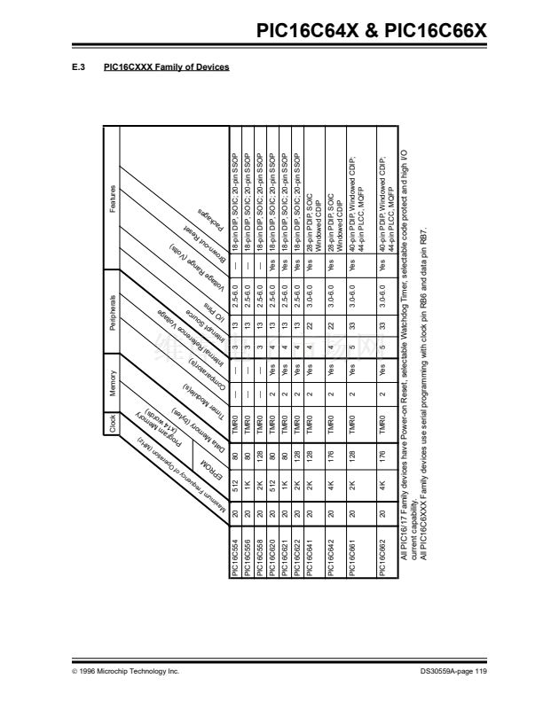
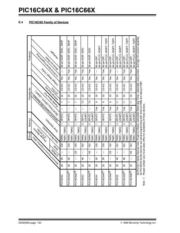
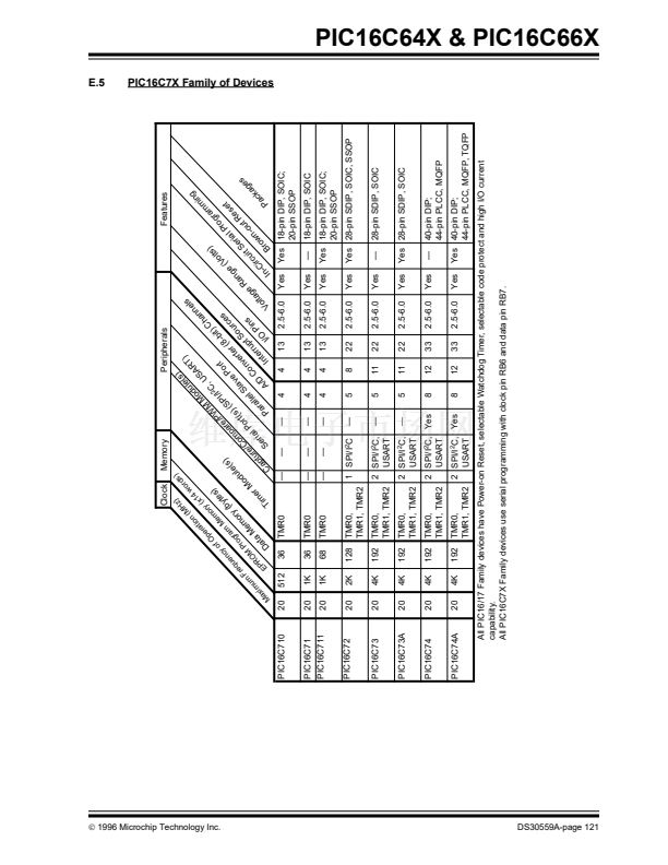
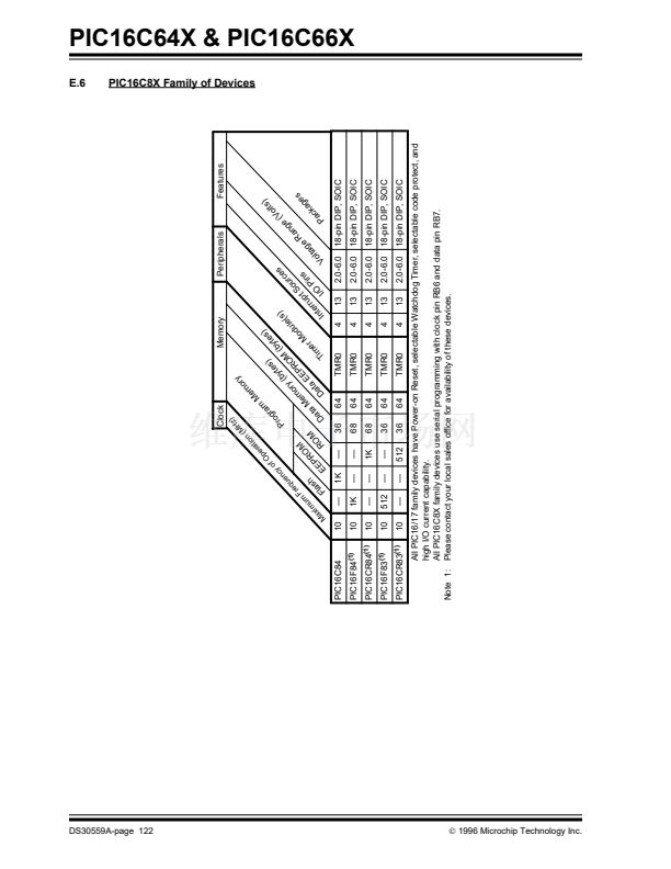
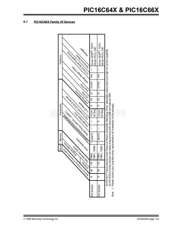
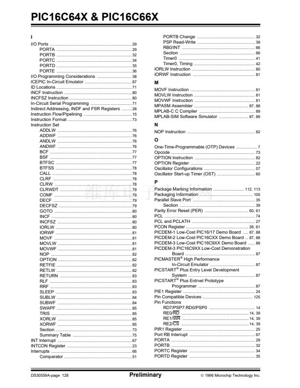
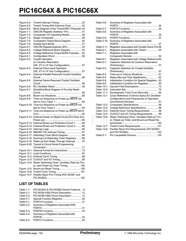
PIC16C64X & PIC16C66X
The code example in Example 7-1 depicts the steps
required to con铿乬ure the comparator module. RA3 and
RA4 are con铿乬ured as digital outputs. RA0 and RA1
are con铿乬ured as the V- inputs and RA2 as the V+ input
to both comparators.
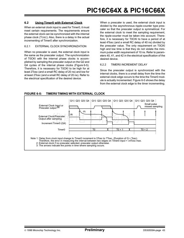
7.3
Comparator Reference
EXAMPLE 7-1:
FLAG_REG
CLRF
CLRF
ANDLW
IORWF
MOVLW
MOVWF
BSF
MOVLW
MOVWF
INITIALIZING THE
COMPARATOR MODULE
;Init Flag Register
;Init PORTA
;Mask Comp bits
;Bits to Flag_Reg
;Init Comp Mode
;CM2:CM0 = 011
;Select Bank 1
;Init Data direction
;RA<2:0> to inputs
;RA<4:3> to outputs
;TRISA<7:5> read '0'
;Select Bank 0
;10
碌
s delay
;Read CMCON to end
;change condition
;Clear Pending Ints
;Select Bank 1
;Enable Comp Ints
;Select Bank 0
;Enable Periph Ints
;Global Int enable
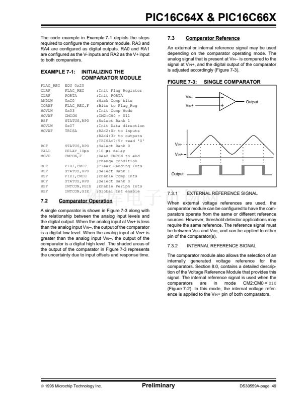
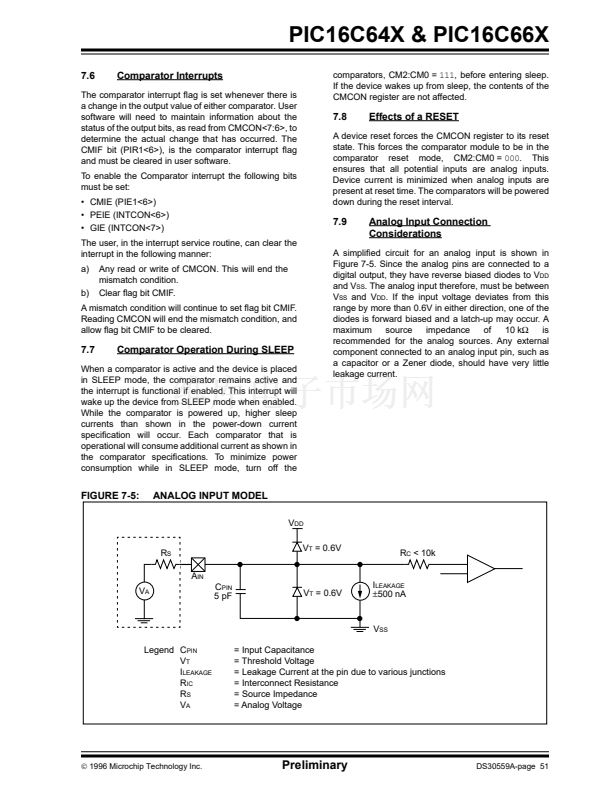
An external or internal reference signal may be used
depending on the comparator operating mode. The
analog signal that is present at V
IN
鈥?is compared to the
signal at V
IN
+, and the digital output of the comparator
is adjusted accordingly (Figure 7-3).
EQU 0x20
FLAG_REG
PORTA
0xC0
FLAG_REG,F
0x03
CMCON
STATUS,RP0
0x07
TRISA
FIGURE 7-3:
V
IN
-
V
IN
+
SINGLE COMPARATOR
Output
BCF
CALL
MOVF
BCF
BSF
BSF
BCF
BSF
BSF
STATUS,RP0
DELAY_10
碌
s
CMCON,F
PIR1,CMIF
STATUS,RP0
PIE1,CMIE
STATUS,RP0
INTCON,PEIE
INTCON,GIE
V
IN
-
V
IN
+
Output
7.3.1
EXTERNAL REFERENCE SIGNAL
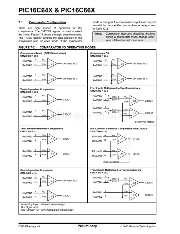
7.2
Comparator Operation
A single comparator is shown in Figure 7-3 along with
the relationship between the analog input levels and
the digital output. When the analog input at V
IN
+ is less
than the analog input V
IN
鈥? the output of the comparator
is a digital low level. When the analog input at V
IN
+ is
greater than the analog input V
IN
鈥? the output of the
comparator is a digital high level. The shaded areas of
the output of the comparator in Figure 7-3 represents
the uncertainty due to input offsets and response time.
When external voltage references are used, the
comparator module can be con铿乬ured to have the com-
parators operate from the same or different reference
sources. However, threshold detector applications may
require the same reference. The reference signal must
be between V
SS
and V
DD
, and can be applied to either
pin of the comparator(s).
7.3.2
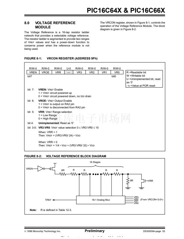
INTERNAL REFERENCE SIGNAL
The comparator module also allows the selection of an
internally generated voltage reference for the
comparators. Section 8.0, contains a detailed descrip-
tion of the Voltage Reference Module that provides this
signal. The internal reference signal is used when the
comparators
are
in
mode
CM2:CM0 =
010
(Figure 7-2). In this mode, the internal voltage refer-
ence is applied to the V
IN
+ pin of both comparators.
漏
1996 Microchip Technology Inc.
Preliminary
DS30559A-page 49


 1
1
 2
2
 3
3
 4
4
 5
5
 6
6
 7
7
 8
8
 9
9
 10
10
 11
11
 12
12
 13
13
 14
14
 15
15
 16
16
 17
17
 18
18
 19
19
 20
20
 21
21
 22
22
 23
23
 24
24
 25
25
 26
26
 27
27
 28
28
 29
29
 30
30
 31
31
 32
32
 33
33
 34
34
 35
35
 36
36
 37
37
 38
38
 39
39
 40
40
 41
41
 42
42
 43
43
 44
44
 45
45
 46
46
 47
47
 48
48
 49
49
 50
50
 51
51
 52
52
 53
53
 54
54
 55
55
 56
56
 57
57
 58
58
 59
59
 60
60
 61
61
 62
62
 63
63
 64
64
 65
65
 66
66
 67
67
 68
68
 69
69
 70
70
 71
71
 72
72
 73
73
 74
74
 75
75
 76
76
 77
77
 78
78
 79
79
 80
80
 81
81
 82
82
 83
83
 84
84
 85
85
 86
86
 87
87
 88
88
 89
89
 90
90
 91
91
 92
92
 93
93
 94
94
 95
95
 96
96
 97
97
 98
98
 99
99
 100
100
 101
101
 102
102
 103
103
 104
104
 105
105
 106
106
 107
107
 108
108
 109
109
 110
110
 111
111
 112
112
 113
113
 114
114
 115
115
 116
116
 117
117
 118
118
 119
119
 120
120
 121
121
 122
122
 123
123
 124
124
 125
125
 126
126
 127
127
 128
128
 129
129
 130
130
 131
131
 132
132
 133
133
 134
134
 135
135
 136
136
