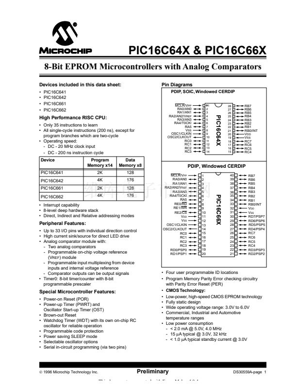
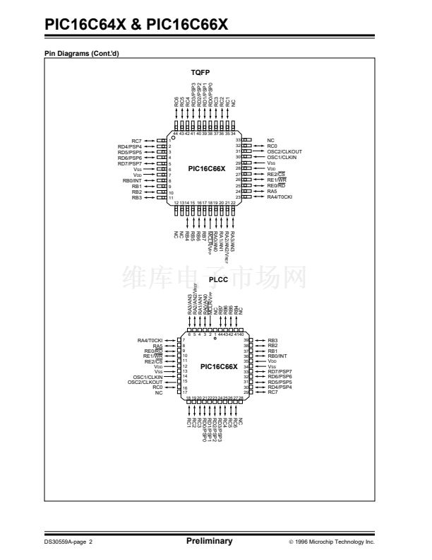
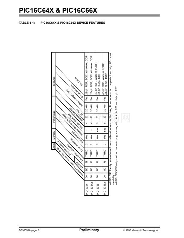
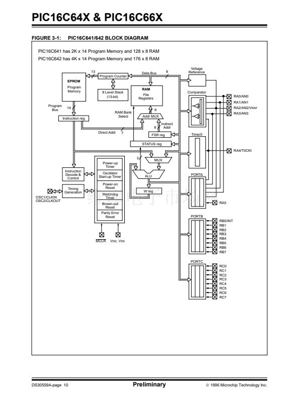
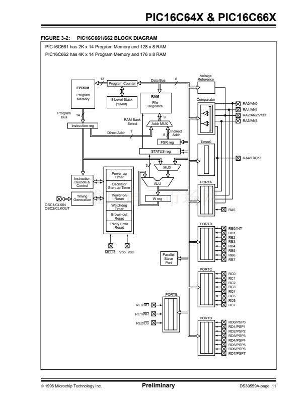
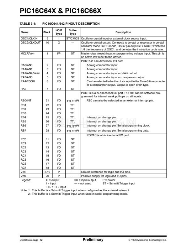
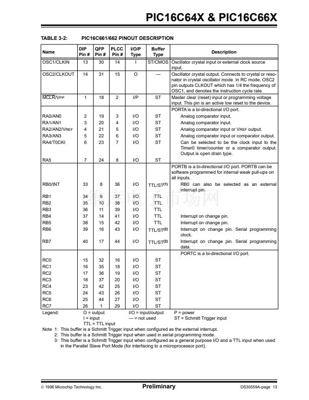
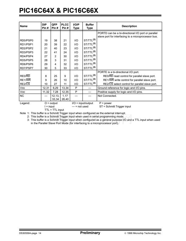
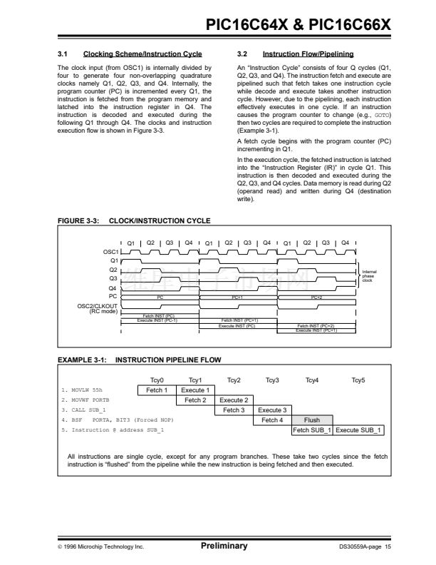
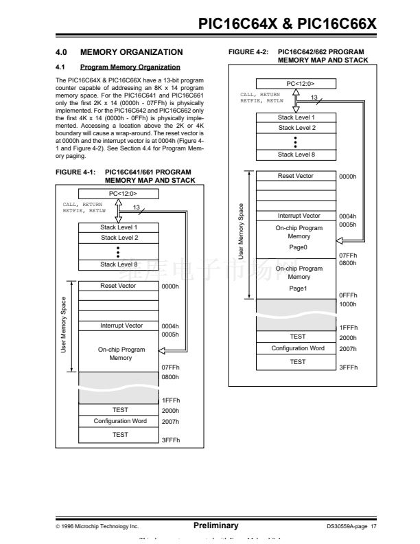
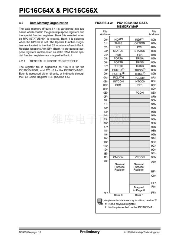
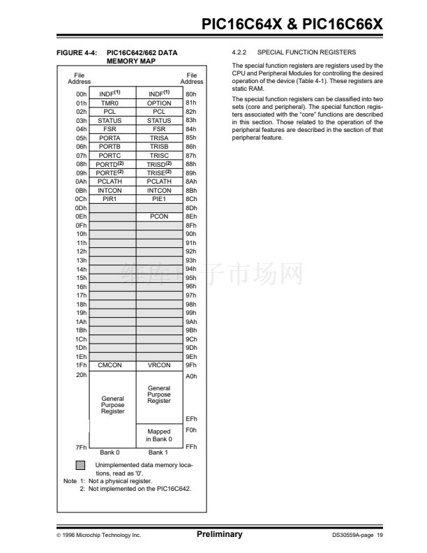
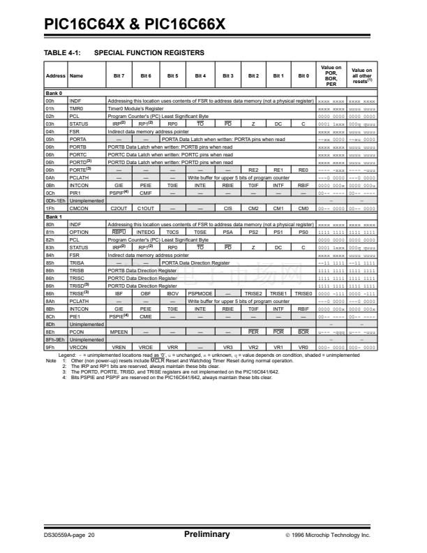
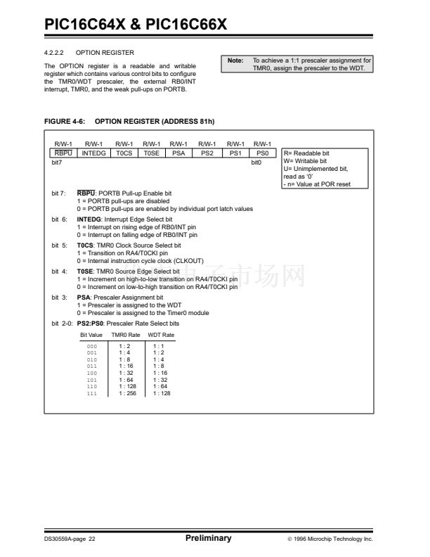
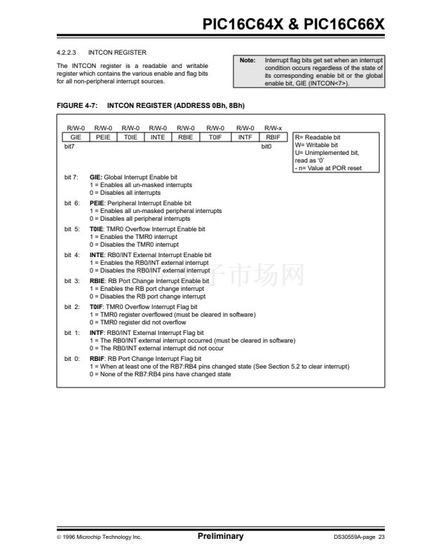
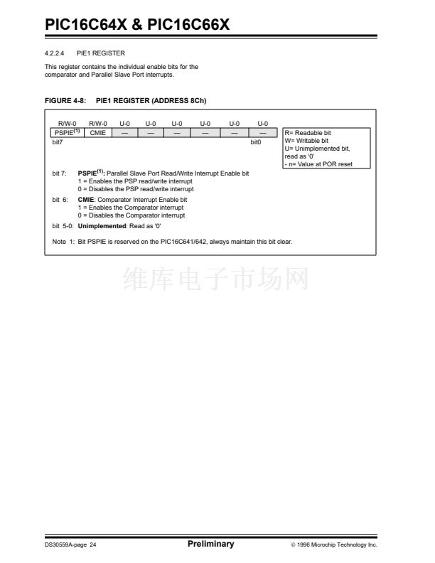
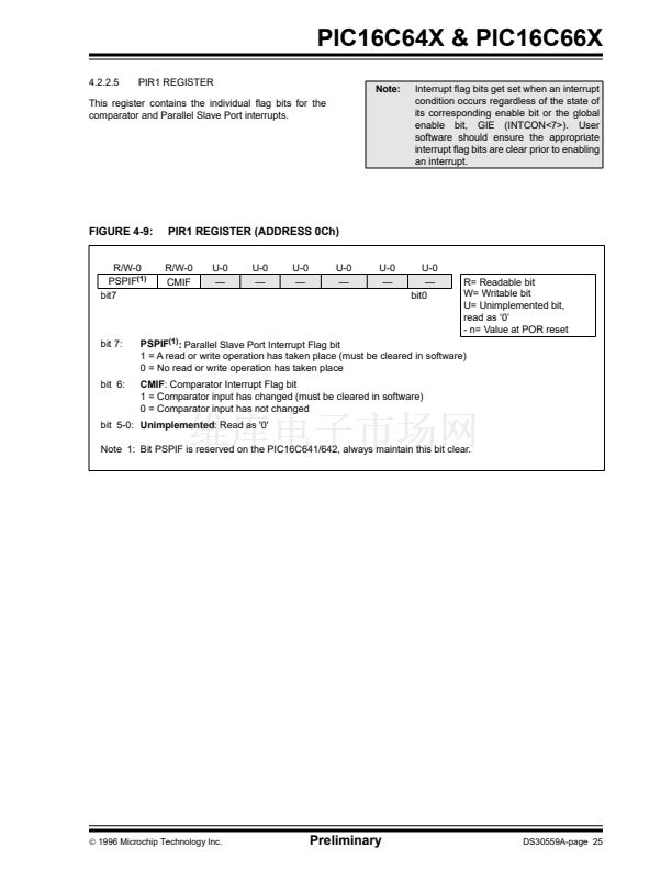
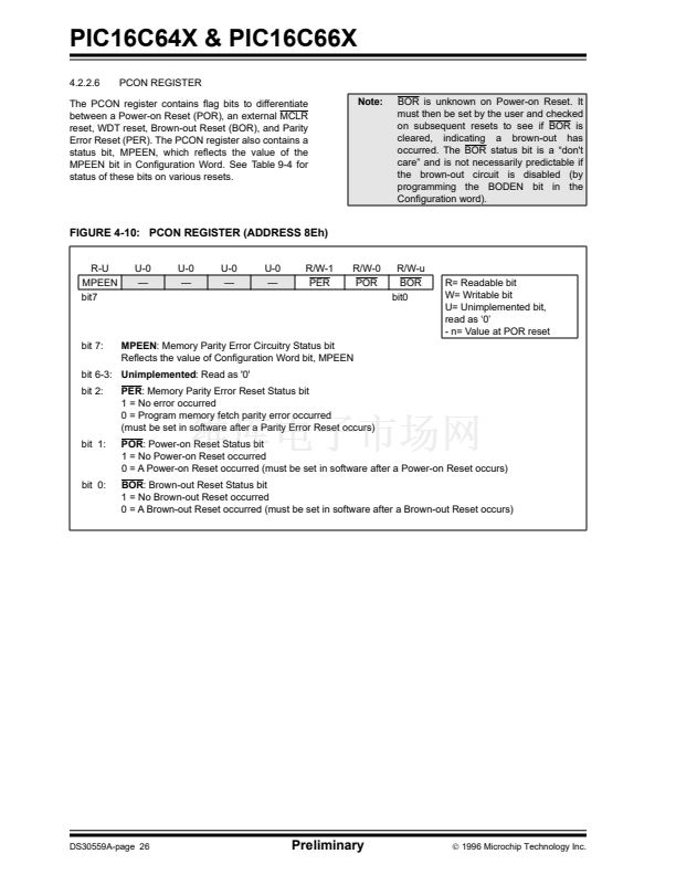
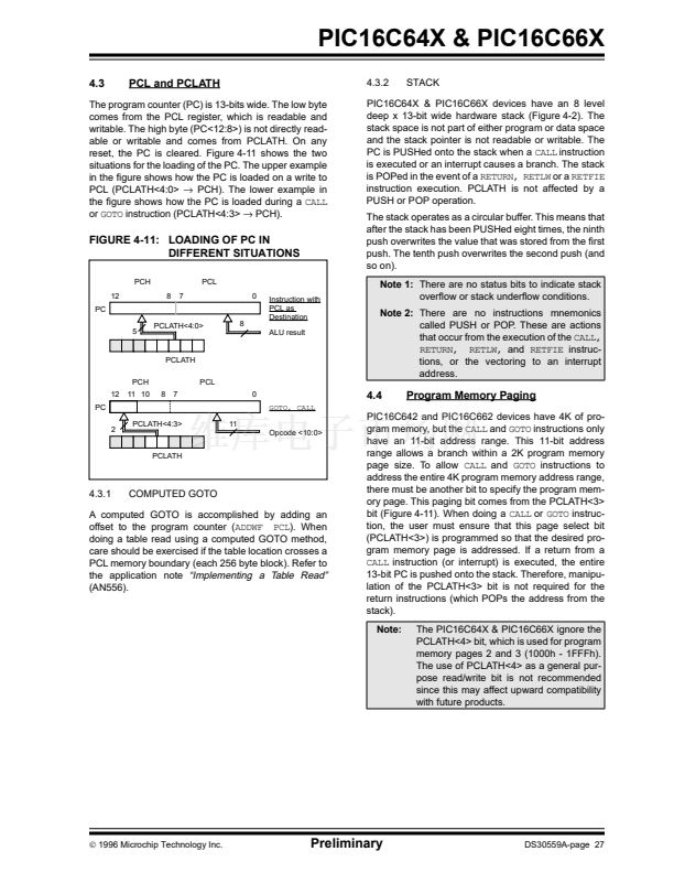
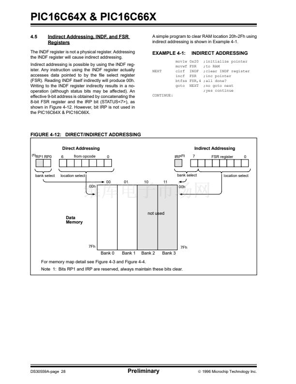
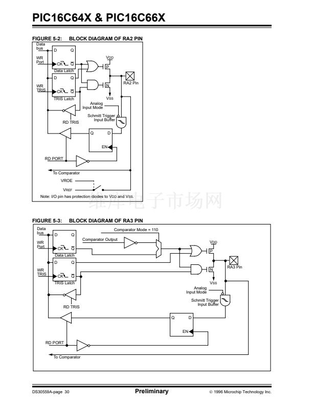
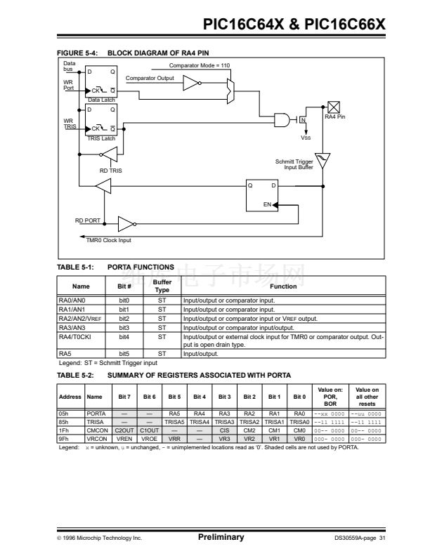
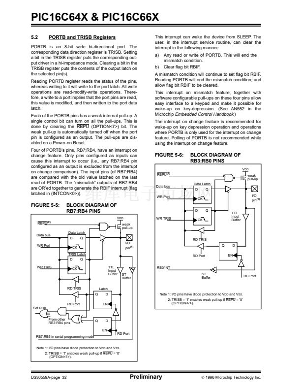
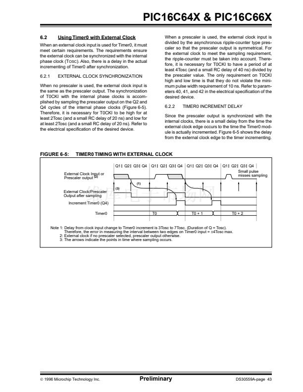
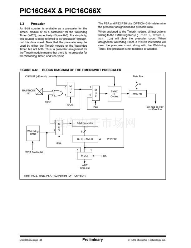
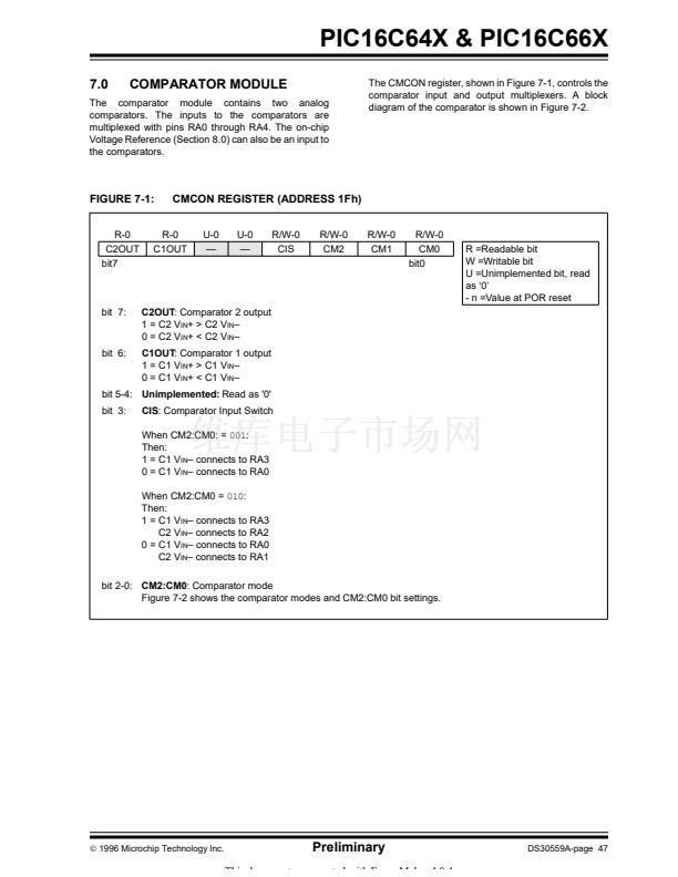
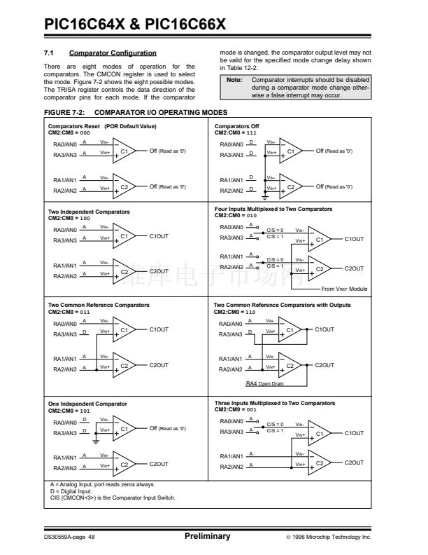
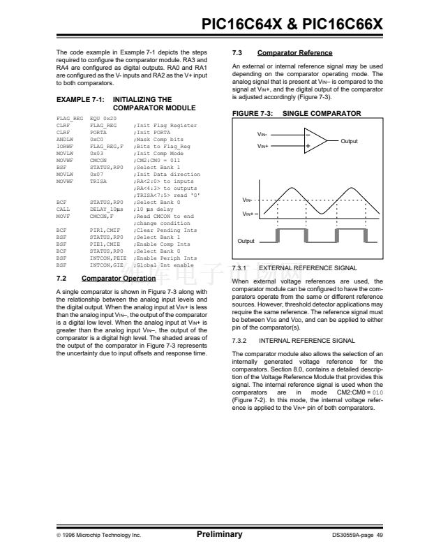
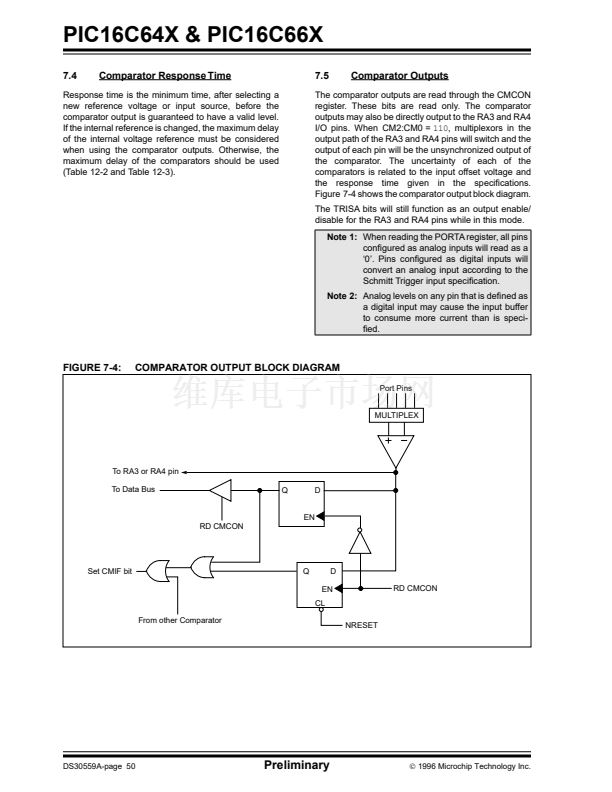
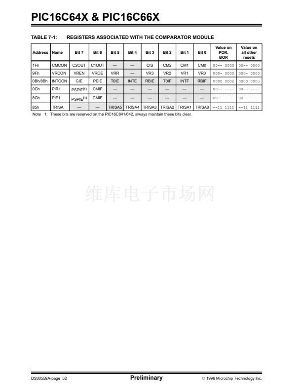
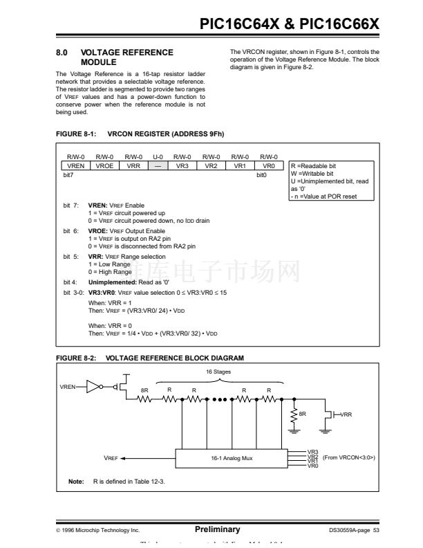
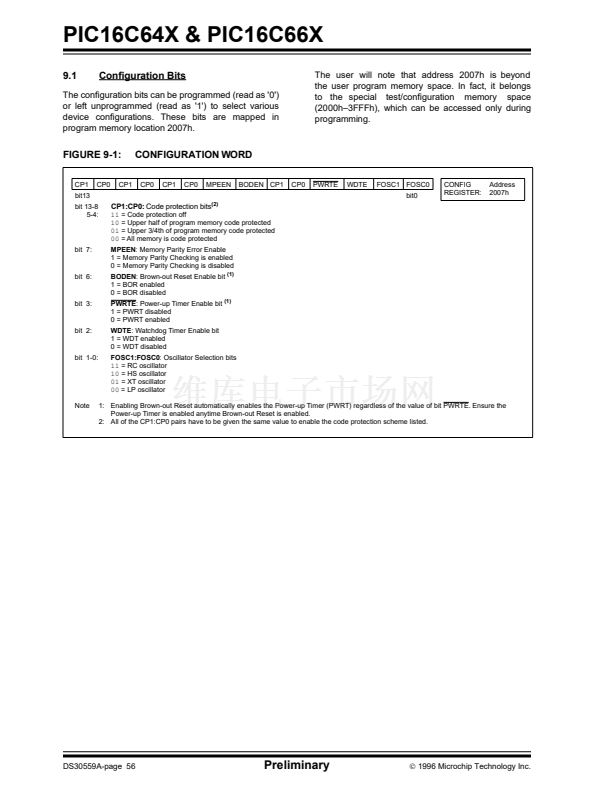
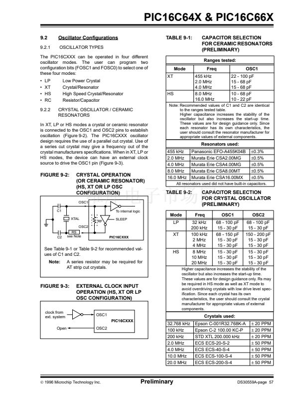
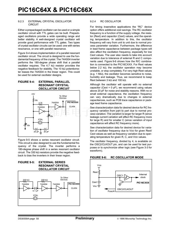
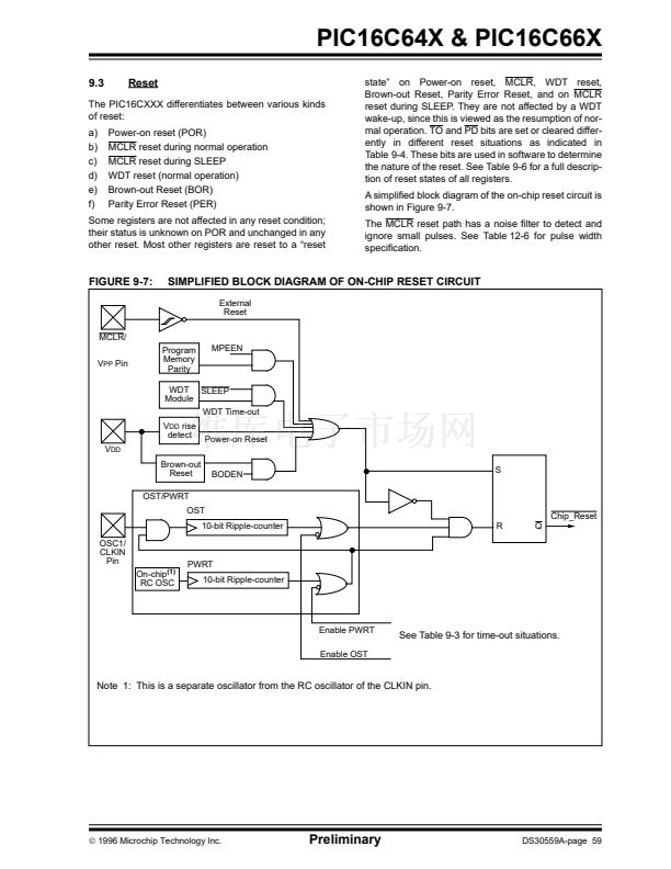
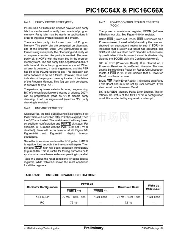
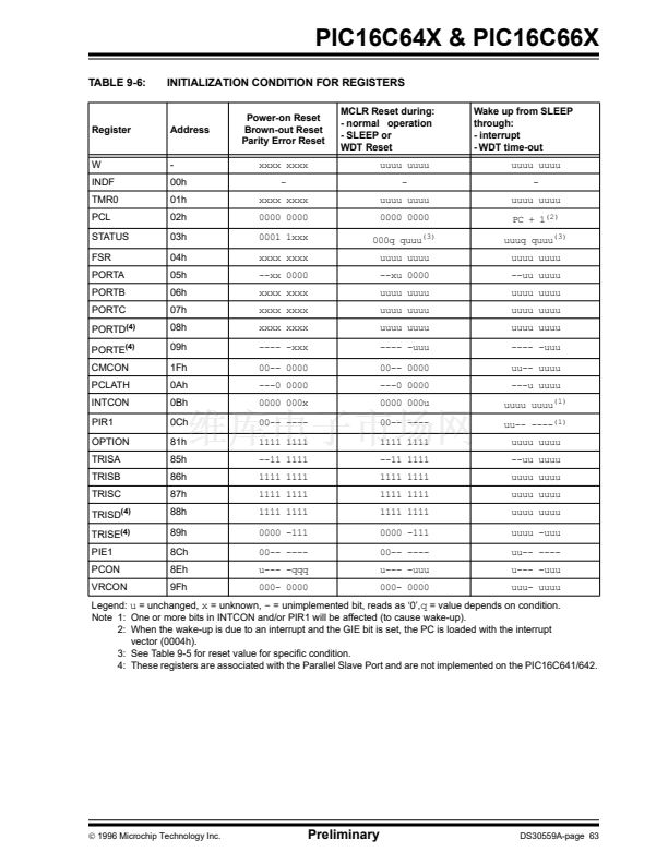
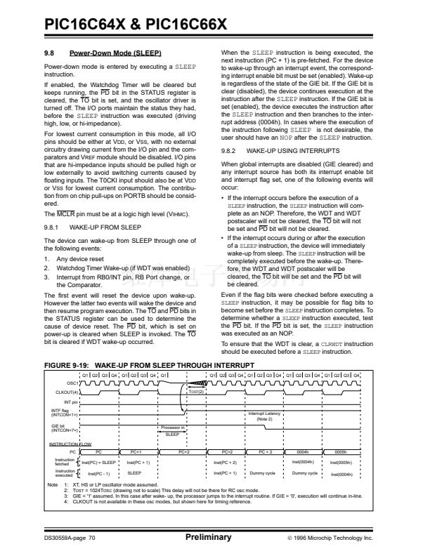
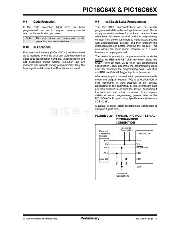
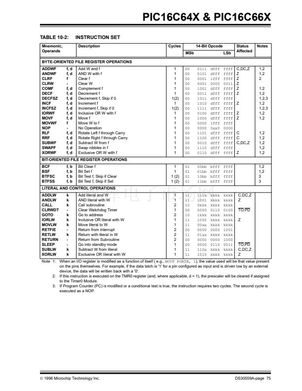
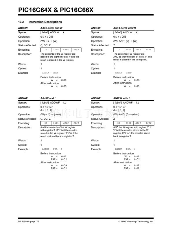
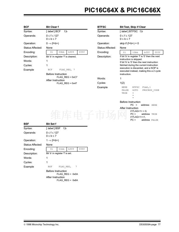
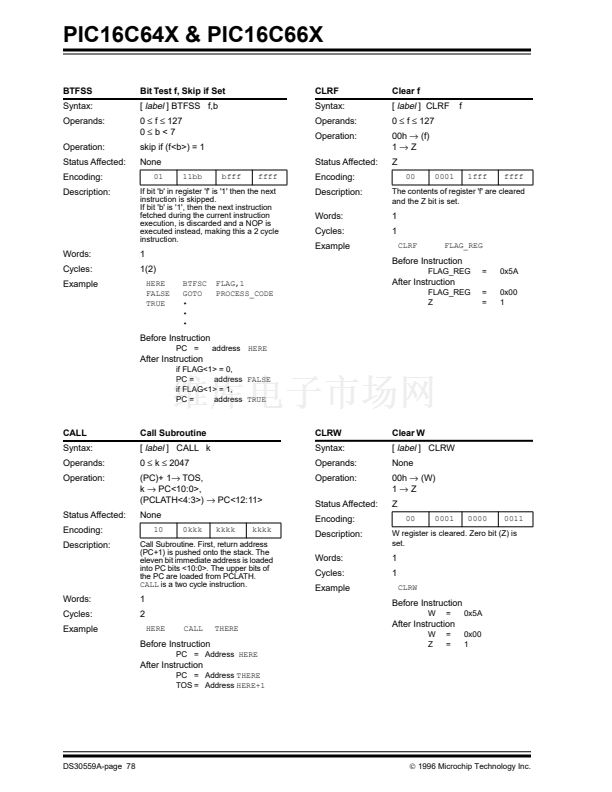
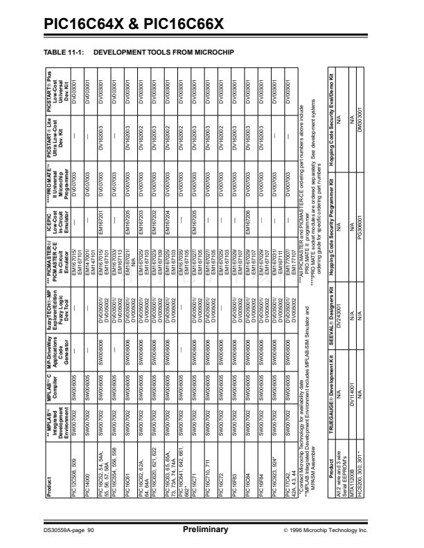
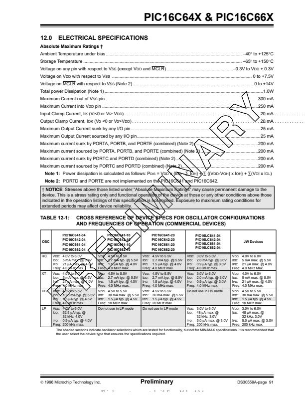
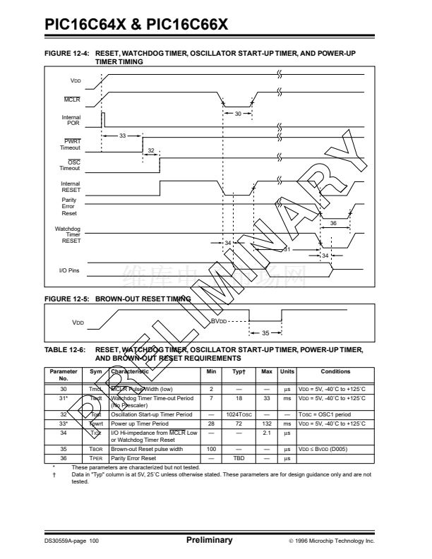
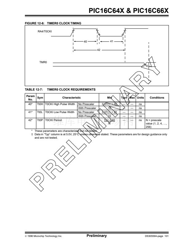
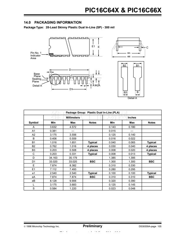
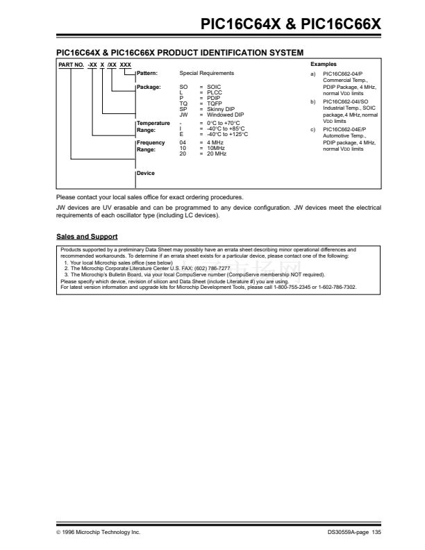
PIC16C64X & PIC16C66X
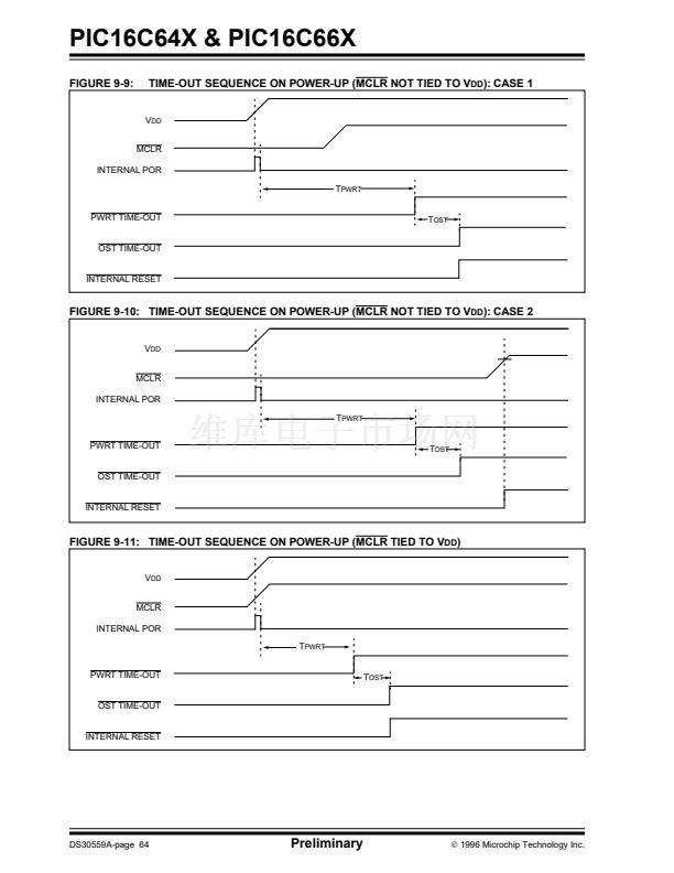
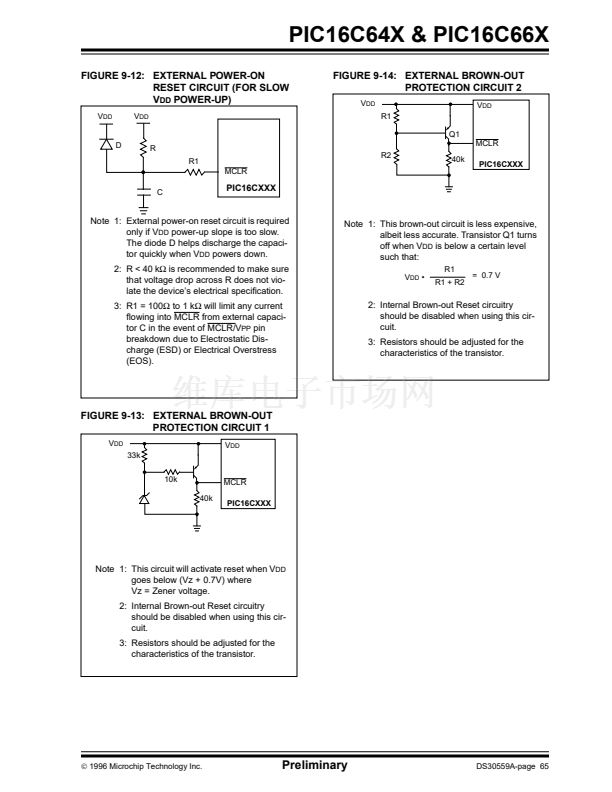
FIGURE 9-12: EXTERNAL POWER-ON
RESET CIRCUIT (FOR SLOW
V
DD
POWER-UP)
V
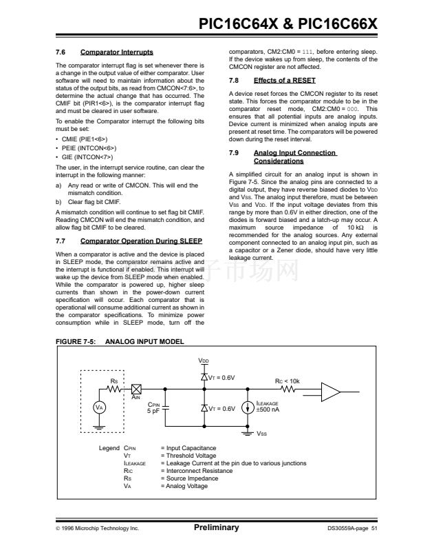
DD
V
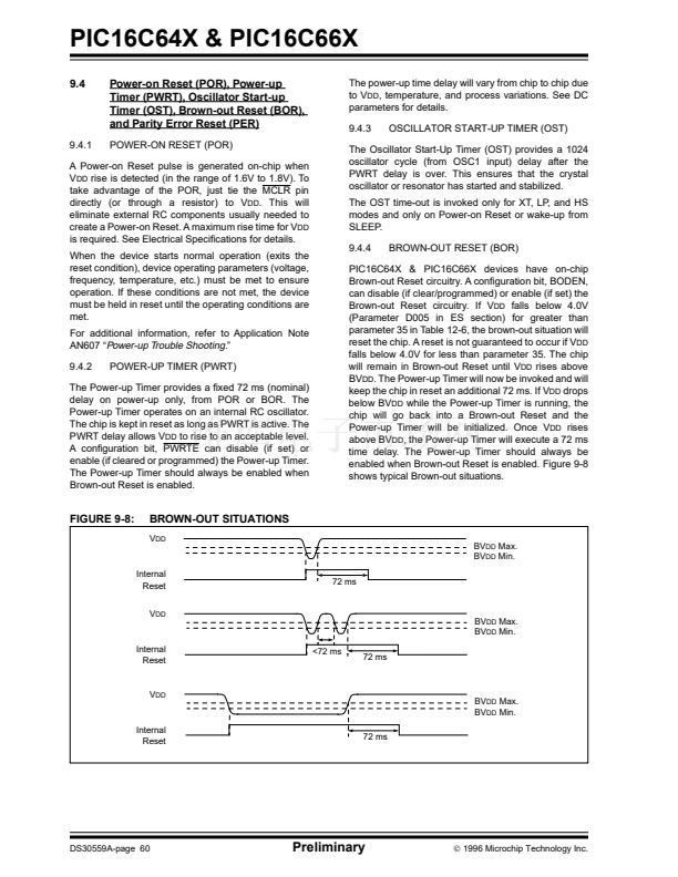
DD
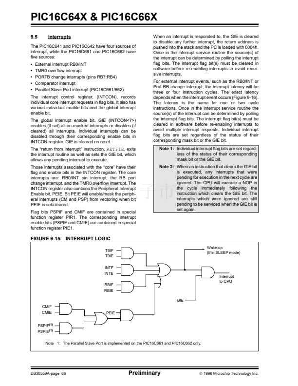
FIGURE 9-14: EXTERNAL BROWN-OUT
PROTECTION CIRCUIT 2
V
DD
R1
Q1
MCLR
V
DD
D
R
R1
MCLR
C
R2
40k
PIC16CXXX
PIC16CXXX
Note 1: External power-on reset circuit is required
only if V
DD
power-up slope is too slow.
The diode D helps discharge the capaci-
tor quickly when V
DD
powers down.
2: R < 40 k鈩?is recommended to make sure
that voltage drop across R does not vio-
late the device鈥檚 electrical speci铿乧ation.
3: R1 = 100鈩?to 1 k鈩?will limit any current
铿俹wing into MCLR from external capaci-
tor C in the event of MCLR/V
PP
pin
breakdown due to Electrostatic Dis-
charge (ESD) or Electrical Overstress
(EOS).
Note 1: This brown-out circuit is less expensive,
albeit less accurate. Transistor Q1 turns
off when V
DD
is below a certain level
such that:
R1
V
DD
鈥?/div>
R1 + R2
= 0.7 V
2: Internal Brown-out Reset circuitry
should be disabled when using this cir-
cuit.
3: Resistors should be adjusted for the
characteristics of the transistor.
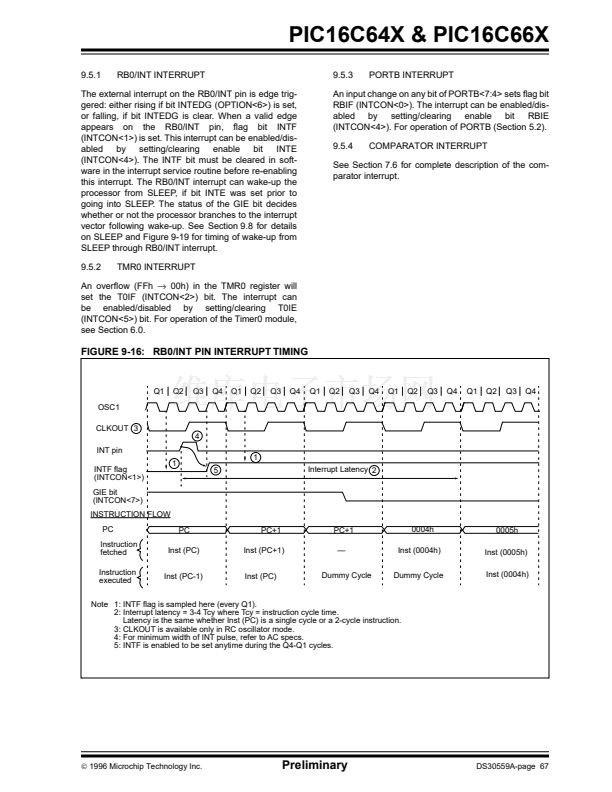
FIGURE 9-13: EXTERNAL BROWN-OUT
PROTECTION CIRCUIT 1
V
DD
33k
10k
40k
MCLR
PIC16CXXX
V
DD
Note 1: This circuit will activate reset when V
DD
goes below (Vz + 0.7V) where
Vz = Zener voltage.
2: Internal Brown-out Reset circuitry
should be disabled when using this cir-
cuit.
3: Resistors should be adjusted for the
characteristics of the transistor.
漏
1996 Microchip Technology Inc.
Preliminary
DS30559A-page 65


 1
1
 2
2
 3
3
 4
4
 5
5
 6
6
 7
7
 8
8
 9
9
 10
10
 11
11
 12
12
 13
13
 14
14
 15
15
 16
16
 17
17
 18
18
 19
19
 20
20
 21
21
 22
22
 23
23
 24
24
 25
25
 26
26
 27
27
 28
28
 29
29
 30
30
 31
31
 32
32
 33
33
 34
34
 35
35
 36
36
 37
37
 38
38
 39
39
 40
40
 41
41
 42
42
 43
43
 44
44
 45
45
 46
46
 47
47
 48
48
 49
49
 50
50
 51
51
 52
52
 53
53
 54
54
 55
55
 56
56
 57
57
 58
58
 59
59
 60
60
 61
61
 62
62
 63
63
 64
64
 65
65
 66
66
 67
67
 68
68
 69
69
 70
70
 71
71
 72
72
 73
73
 74
74
 75
75
 76
76
 77
77
 78
78
 79
79
 80
80
 81
81
 82
82
 83
83
 84
84
 85
85
 86
86
 87
87
 88
88
 89
89
 90
90
 91
91
 92
92
 93
93
 94
94
 95
95
 96
96
 97
97
 98
98
 99
99
 100
100
 101
101
 102
102
 103
103
 104
104
 105
105
 106
106
 107
107
 108
108
 109
109
 110
110
 111
111
 112
112
 113
113
 114
114
 115
115
 116
116
 117
117
 118
118
 119
119
 120
120
 121
121
 122
122
 123
123
 124
124
 125
125
 126
126
 127
127
 128
128
 129
129
 130
130
 131
131
 132
132
 133
133
 134
134
 135
135
 136
136
