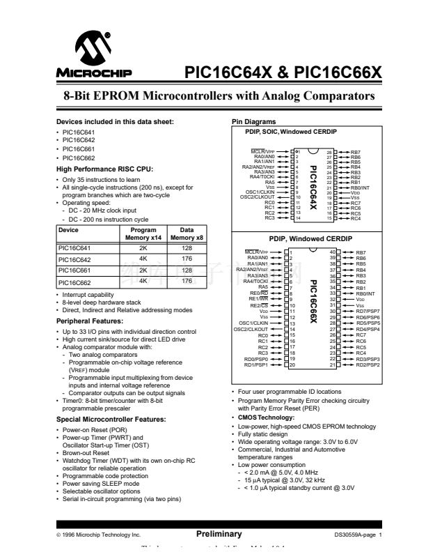
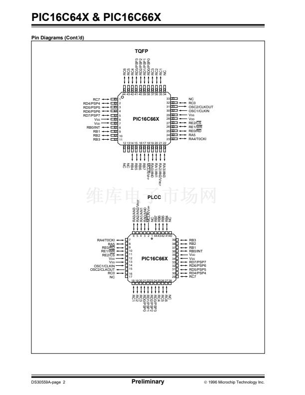
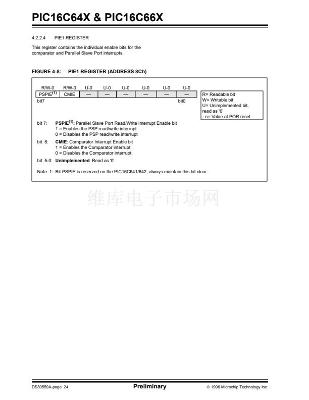
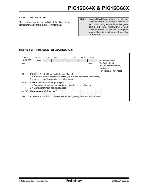
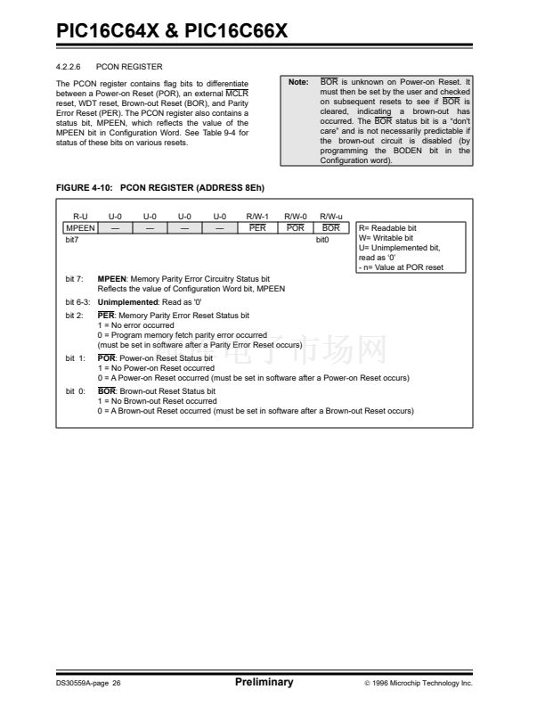
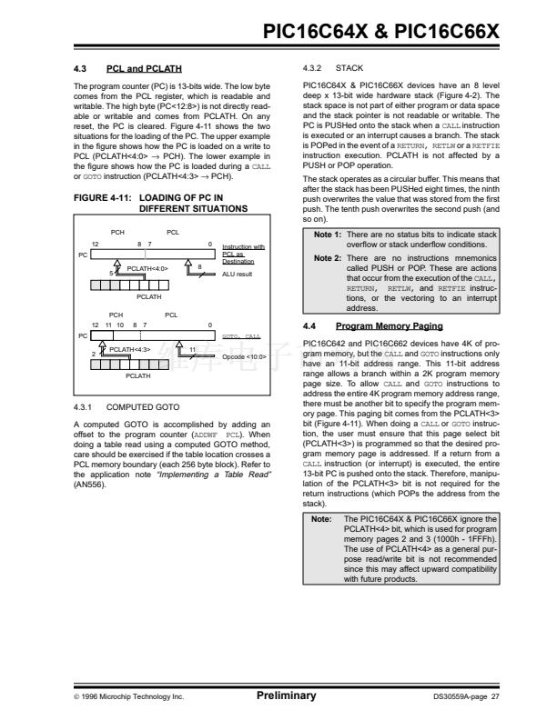
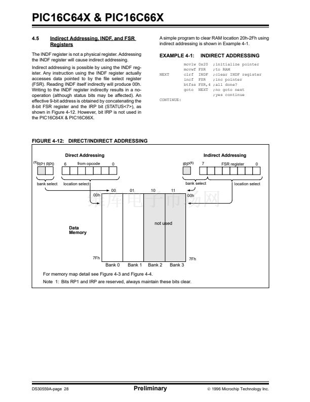
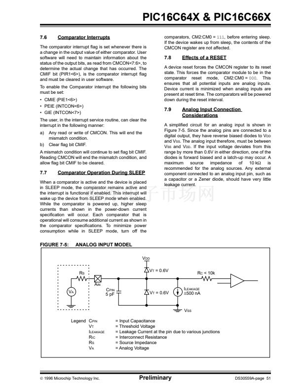
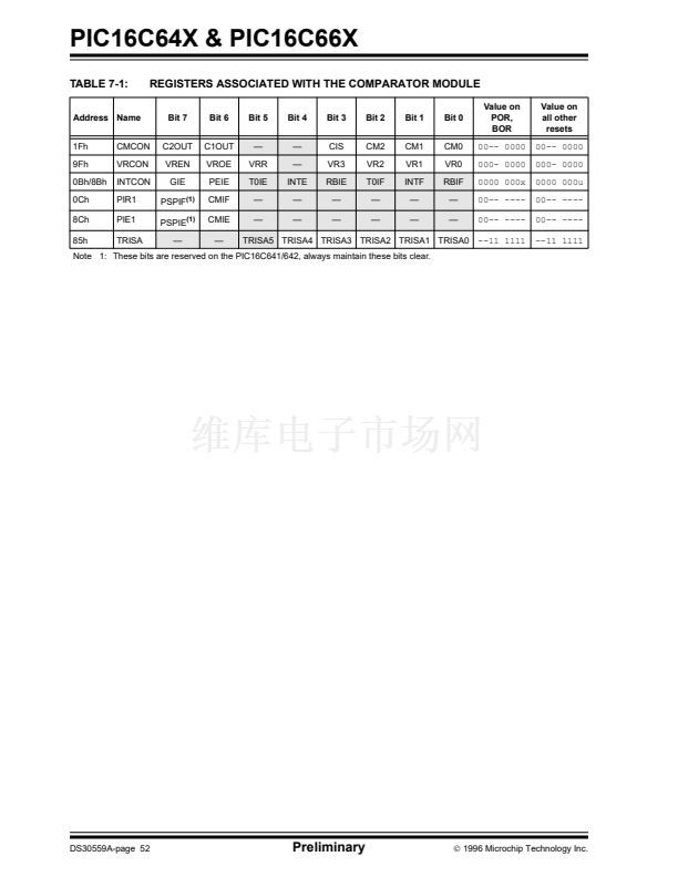
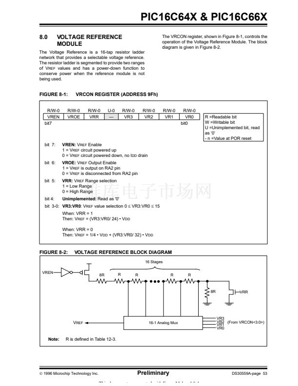
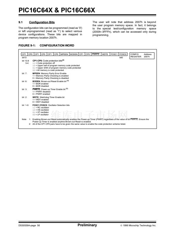
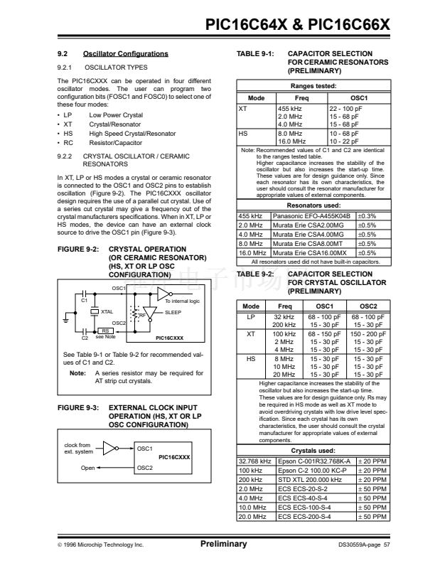
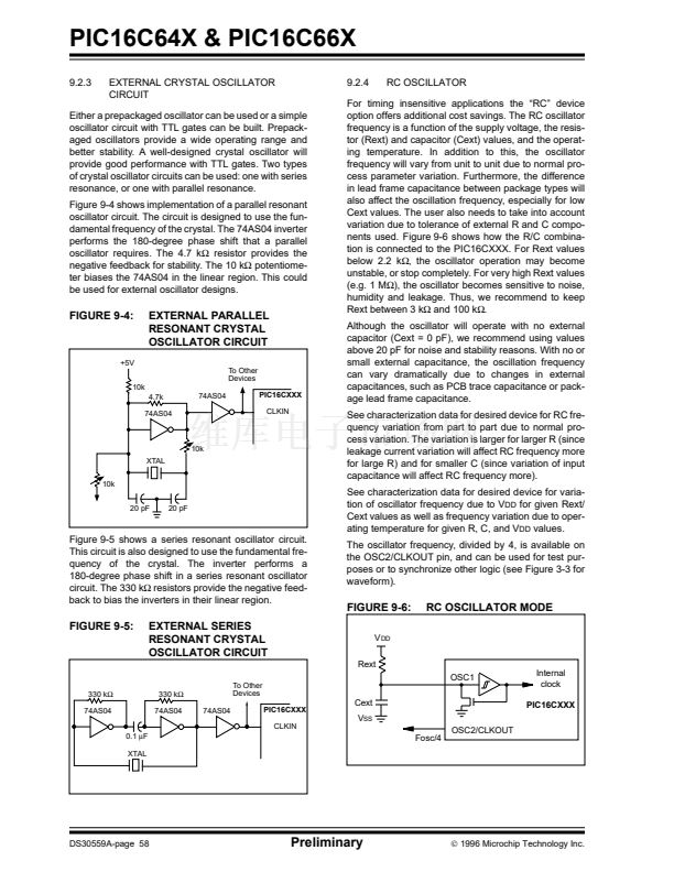
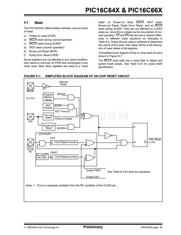
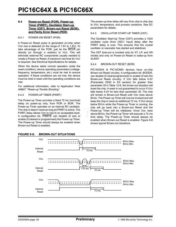
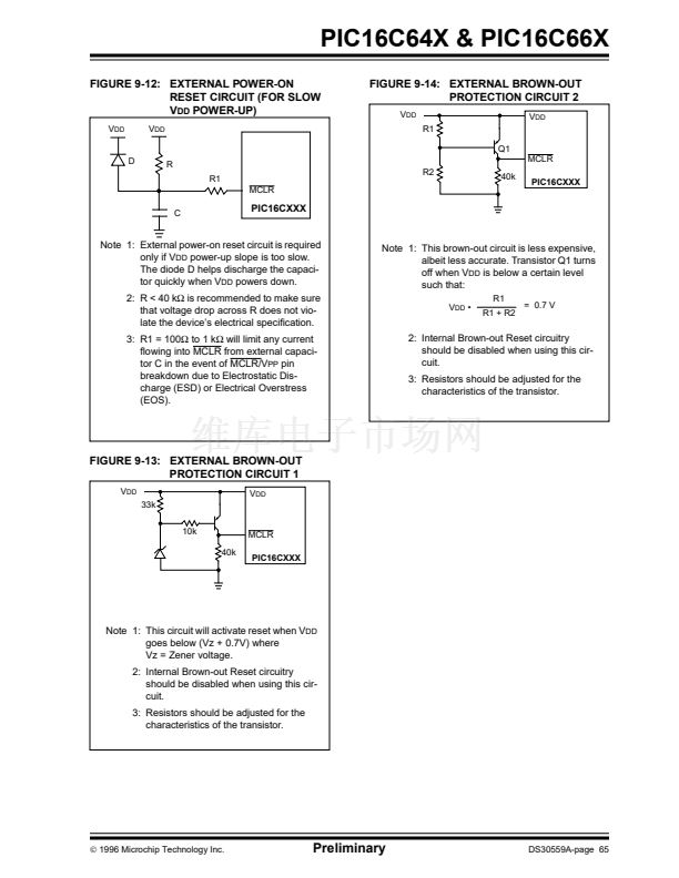
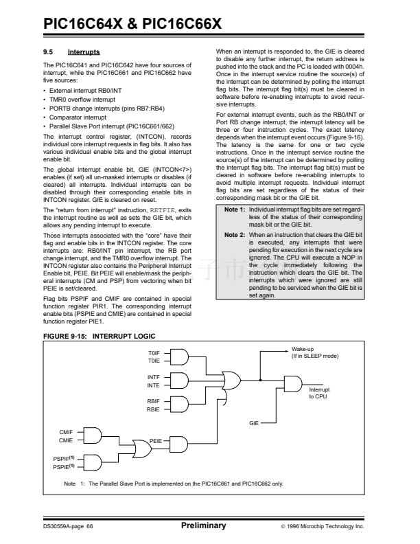
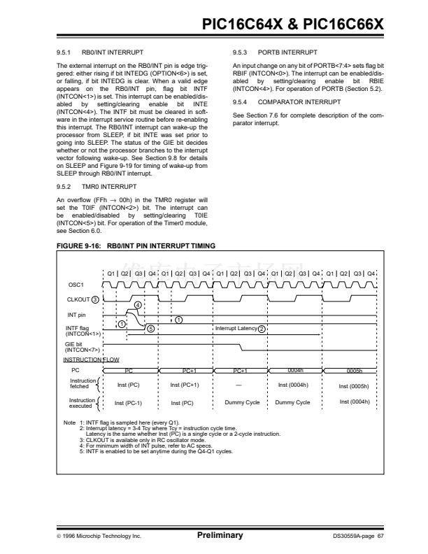
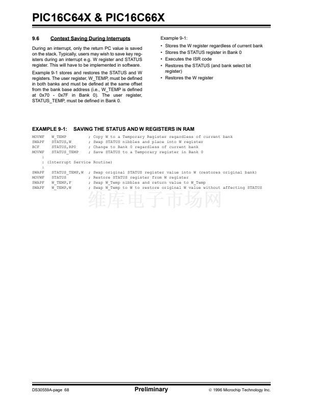
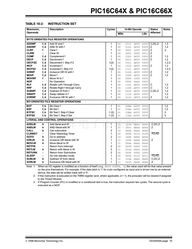
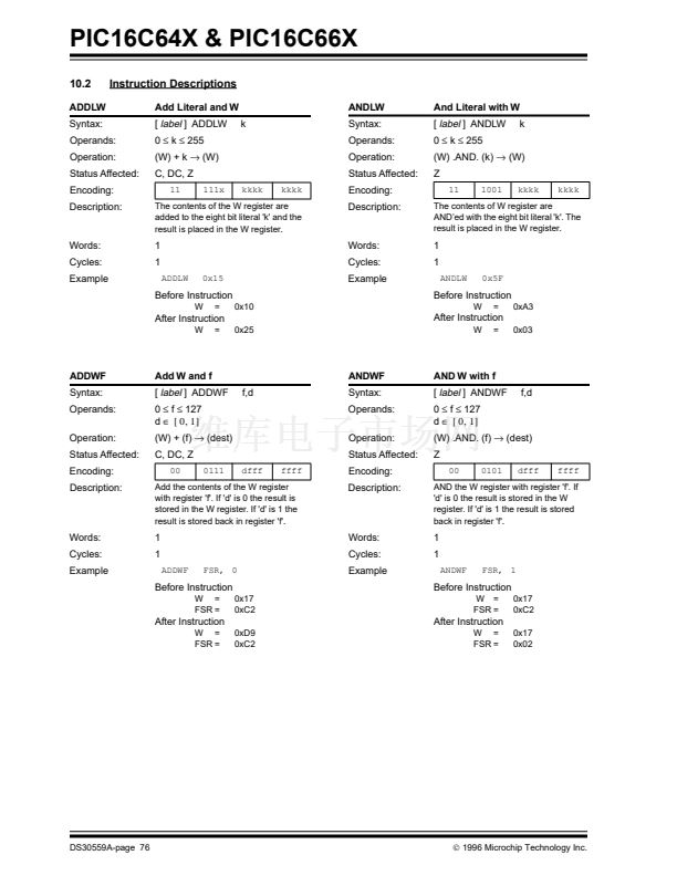
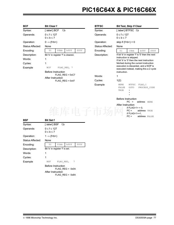
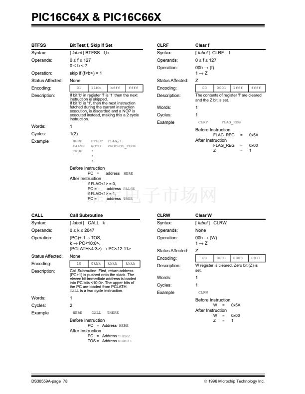
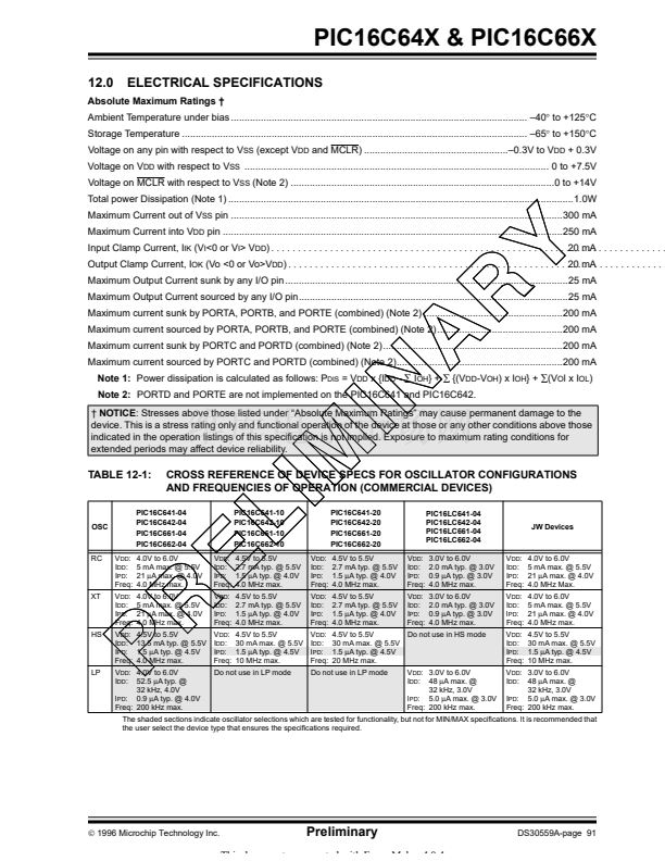
鈮?/div>
V
DD
, XT, HS and LP
osc con铿乬uration
I
OL
= 8.5 mA, V
DD
= 4.5V,
-40掳 to +85掳C
I
OL
= 7.0
M
A, V
DD
= 4.5V, +125掳C
I
OL
= 1.6 mA, V
DD
= 4.5V,
-40掳 to +85掳C
I
OL
= 1.2 mA, V
DD
= 4.5V, +125掳C
-
-
-
-
-
-
0.6
0.6
0.6
V
V
V
D083
OSC2/CLKOUT
(RC only)
-
-
0.6
V
* These parameters are characterized but not tested.
鈥?Data in 鈥淭yp鈥?column is at 5.0V, 25掳C unless otherwise stated. These parameters are for design guidance only and
are not tested.
Note 1: In RC oscillator con铿乬uration, the OSC1 pin is a Schmitt Trigger input. It is not recommended that the
PIC16C64X & PIC16C66X be driven with external clock in RC mode.
2: The leakage current on the MCLR pin is strongly dependent on applied voltage level. The speci铿乪d levels repre-
sent normal operating conditions. Higher leakage current may be measured at different input voltages.
3: Negative current is de铿乶ed as coming out of the pin.
DS30559A-page 94
Preliminary
漏
1996 Microchip Technology Inc.


 1
1
 2
2
 3
3
 4
4
 5
5
 6
6
 7
7
 8
8
 9
9
 10
10
 11
11
 12
12
 13
13
 14
14
 15
15
 16
16
 17
17
 18
18
 19
19
 20
20
 21
21
 22
22
 23
23
 24
24
 25
25
 26
26
 27
27
 28
28
 29
29
 30
30
 31
31
 32
32
 33
33
 34
34
 35
35
 36
36
 37
37
 38
38
 39
39
 40
40
 41
41
 42
42
 43
43
 44
44
 45
45
 46
46
 47
47
 48
48
 49
49
 50
50
 51
51
 52
52
 53
53
 54
54
 55
55
 56
56
 57
57
 58
58
 59
59
 60
60
 61
61
 62
62
 63
63
 64
64
 65
65
 66
66
 67
67
 68
68
 69
69
 70
70
 71
71
 72
72
 73
73
 74
74
 75
75
 76
76
 77
77
 78
78
 79
79
 80
80
 81
81
 82
82
 83
83
 84
84
 85
85
 86
86
 87
87
 88
88
 89
89
 90
90
 91
91
 92
92
 93
93
 94
94
 95
95
 96
96
 97
97
 98
98
 99
99
 100
100
 101
101
 102
102
 103
103
 104
104
 105
105
 106
106
 107
107
 108
108
 109
109
 110
110
 111
111
 112
112
 113
113
 114
114
 115
115
 116
116
 117
117
 118
118
 119
119
 120
120
 121
121
 122
122
 123
123
 124
124
 125
125
 126
126
 127
127
 128
128
 129
129
 130
130
 131
131
 132
132
 133
133
 134
134
 135
135
 136
136
