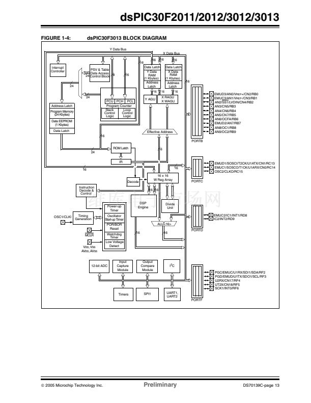
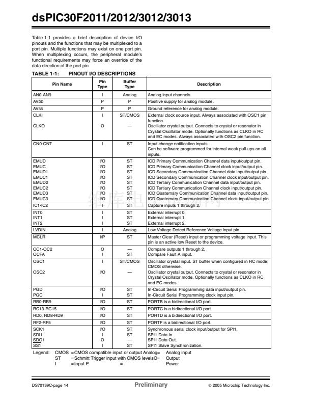
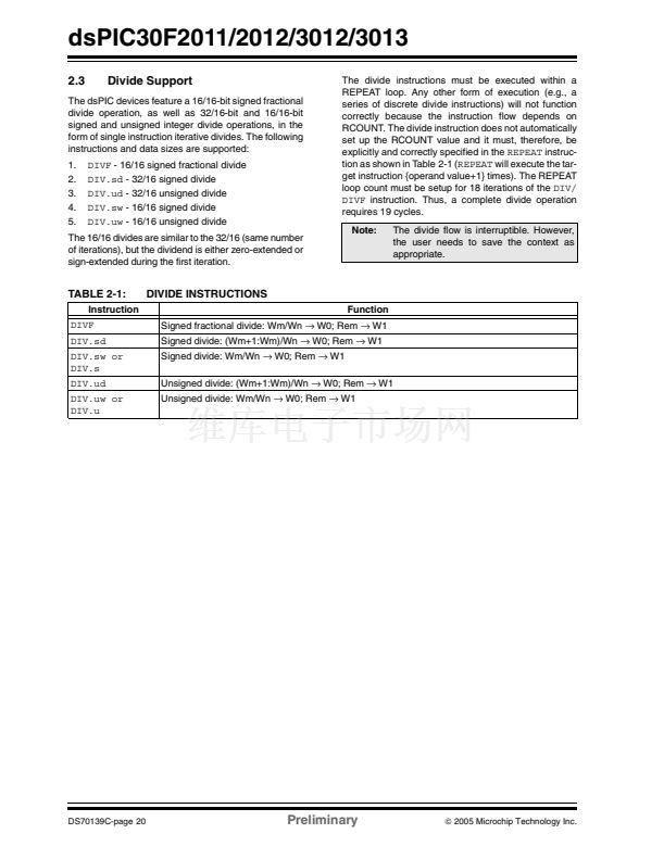
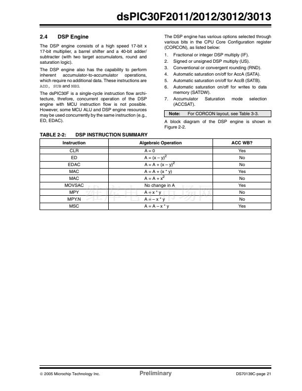
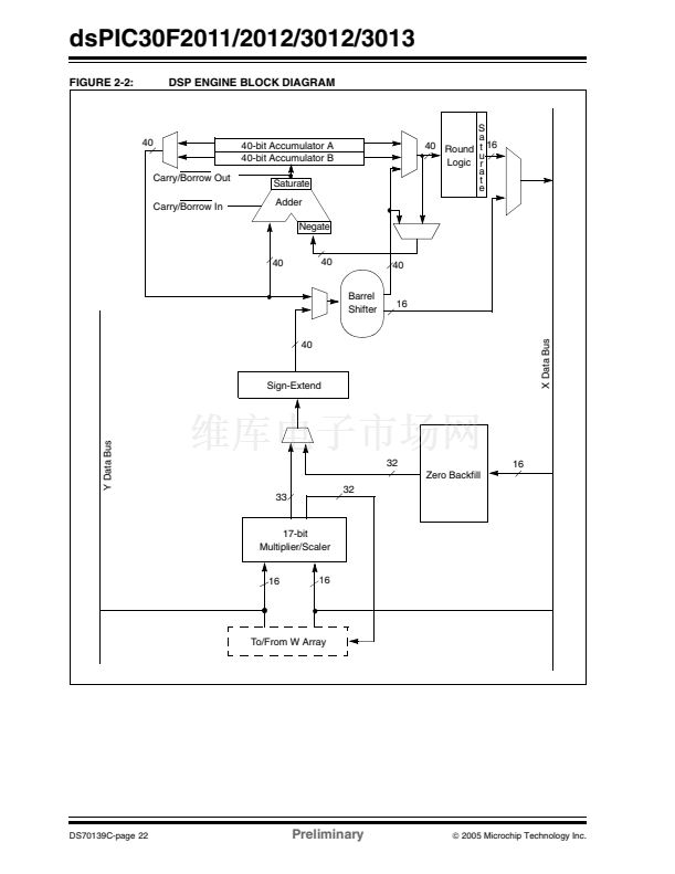
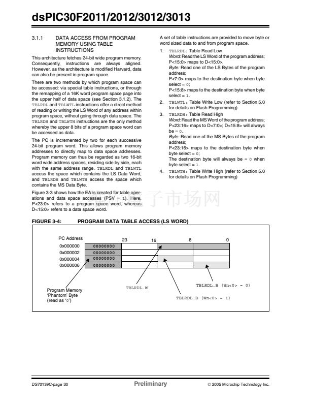
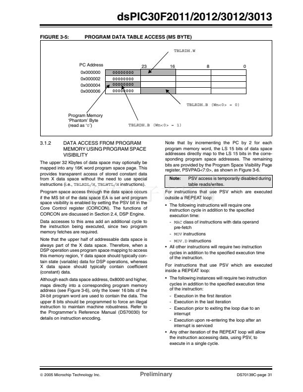
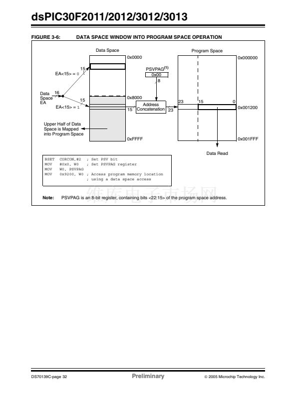
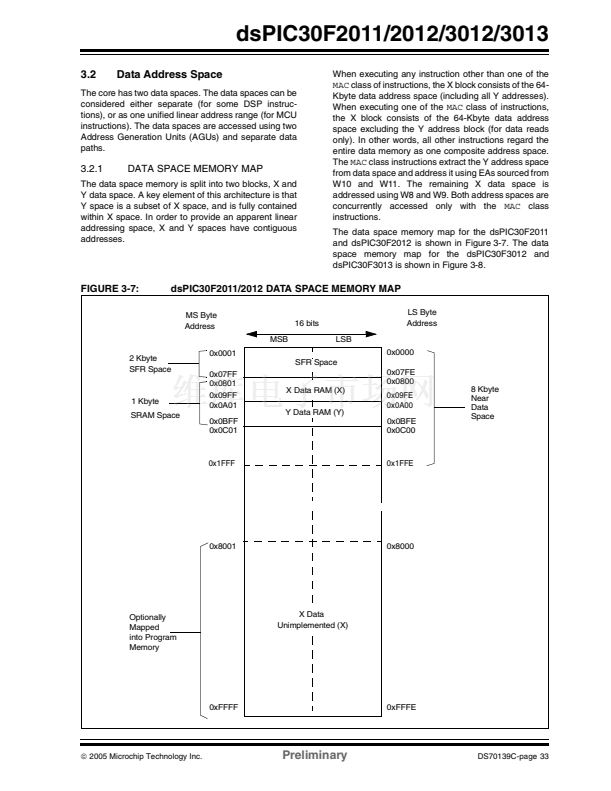
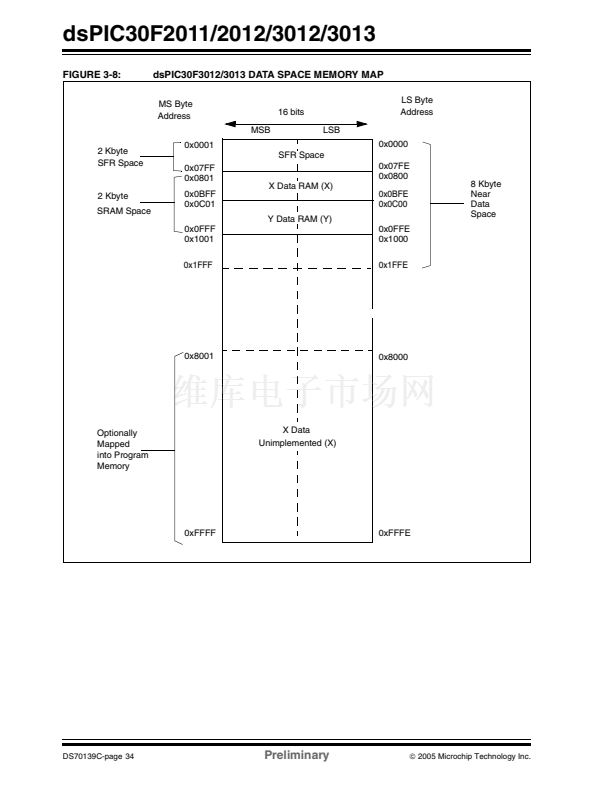
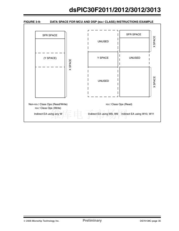
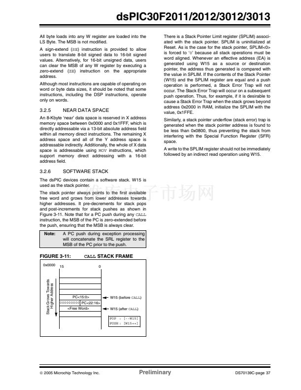
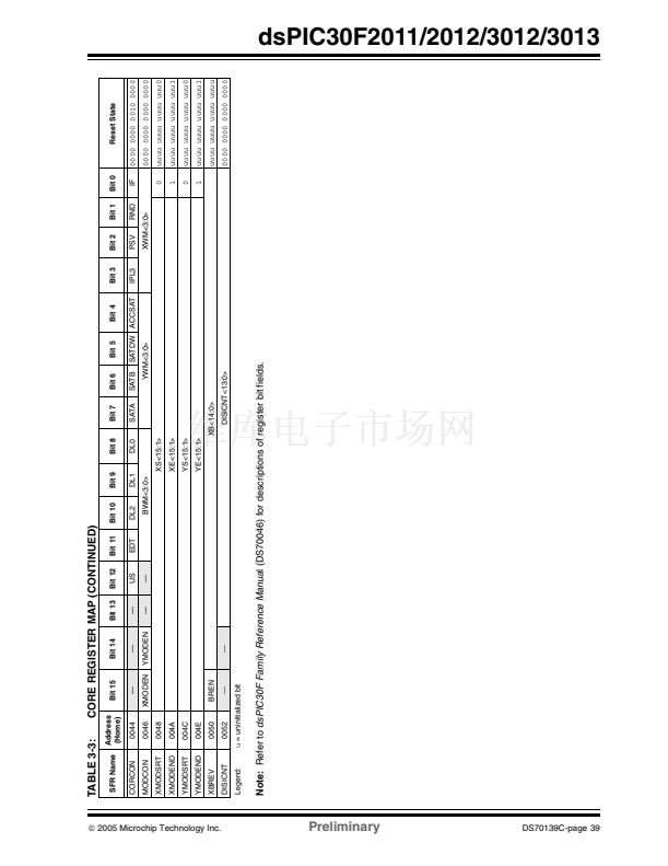
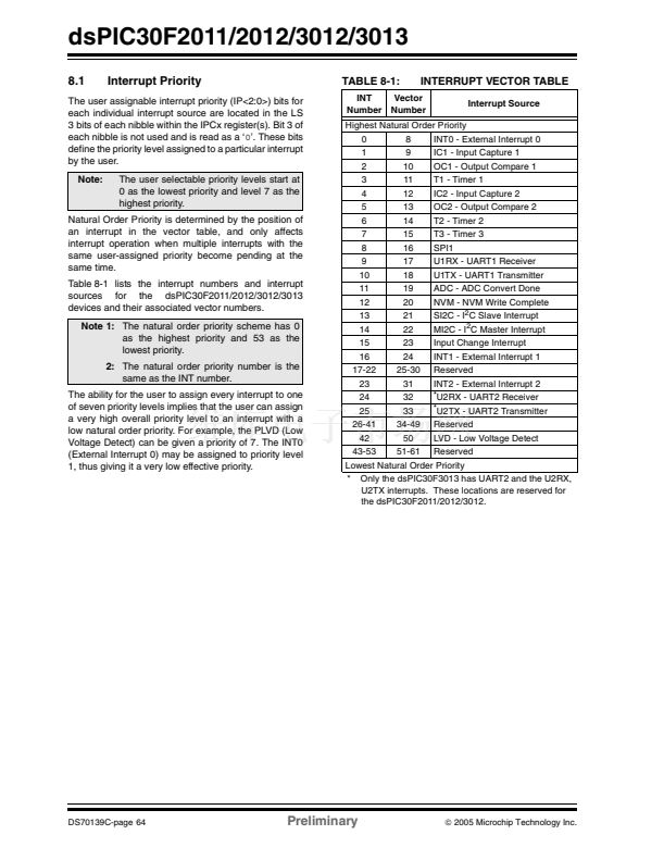
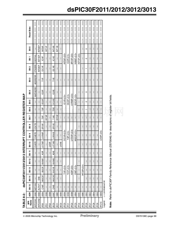
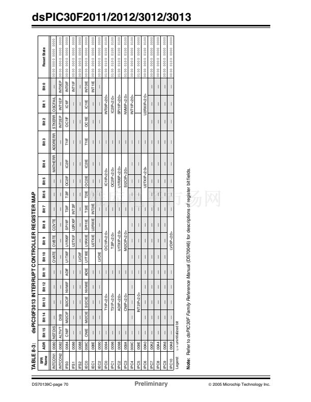
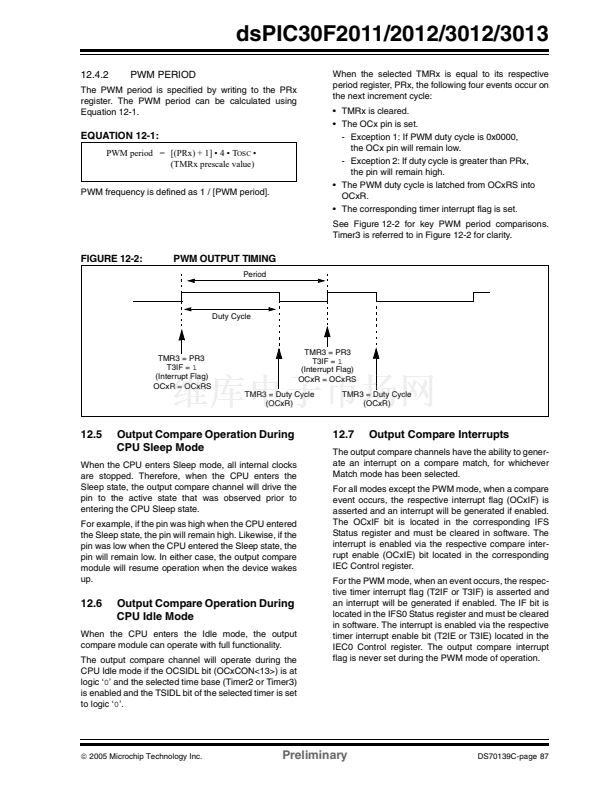
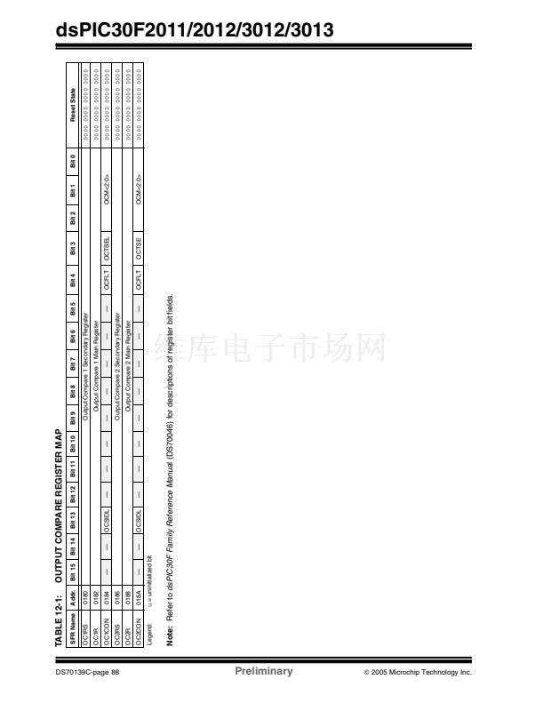
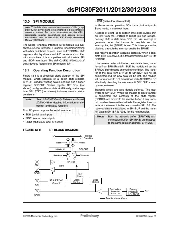
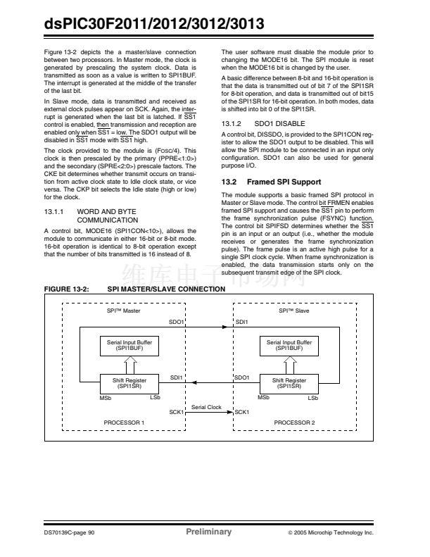
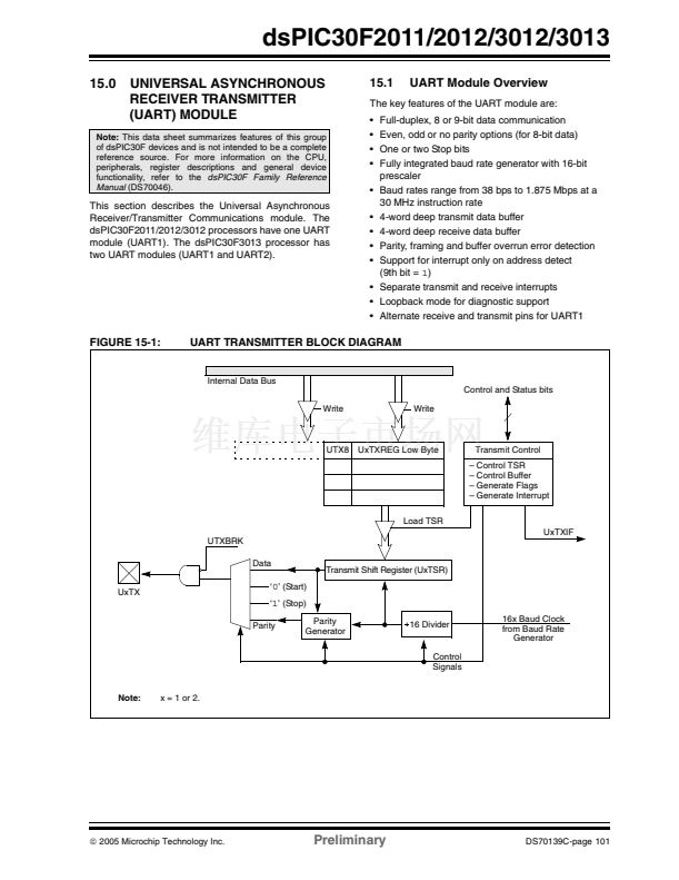
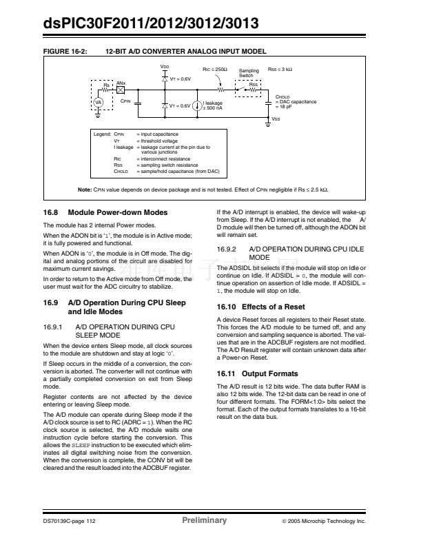
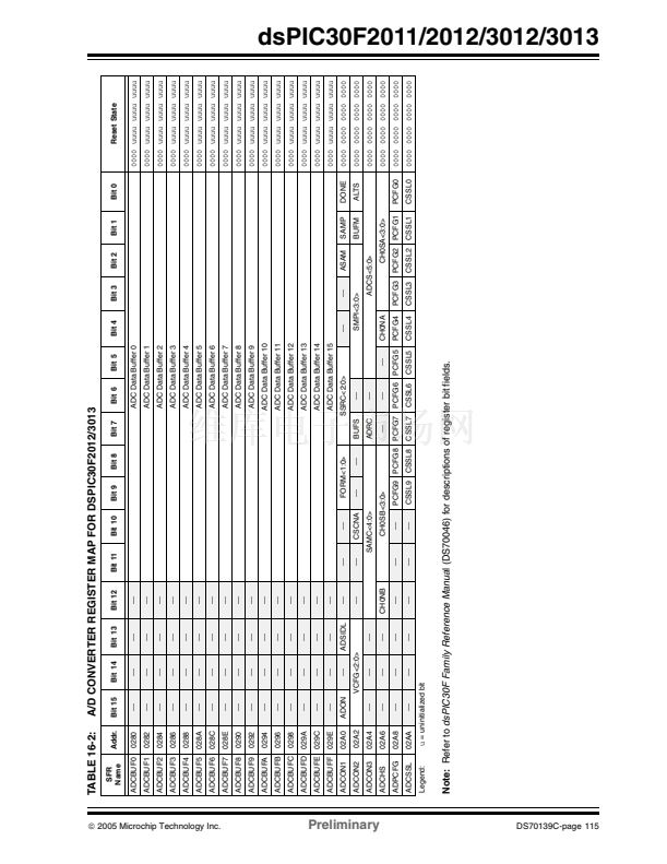
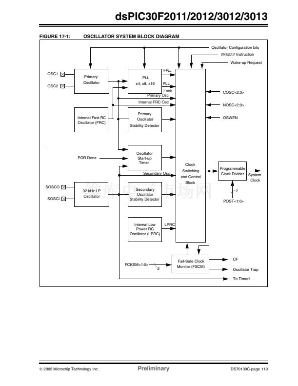
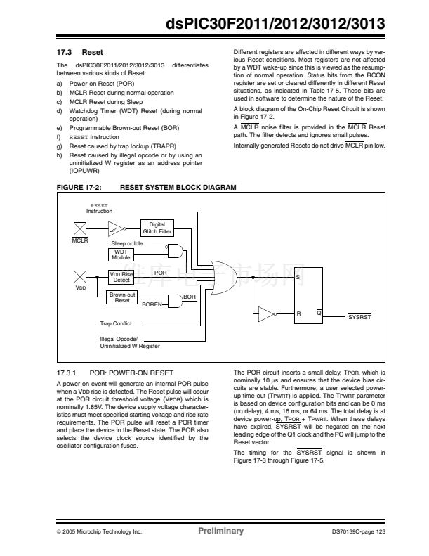
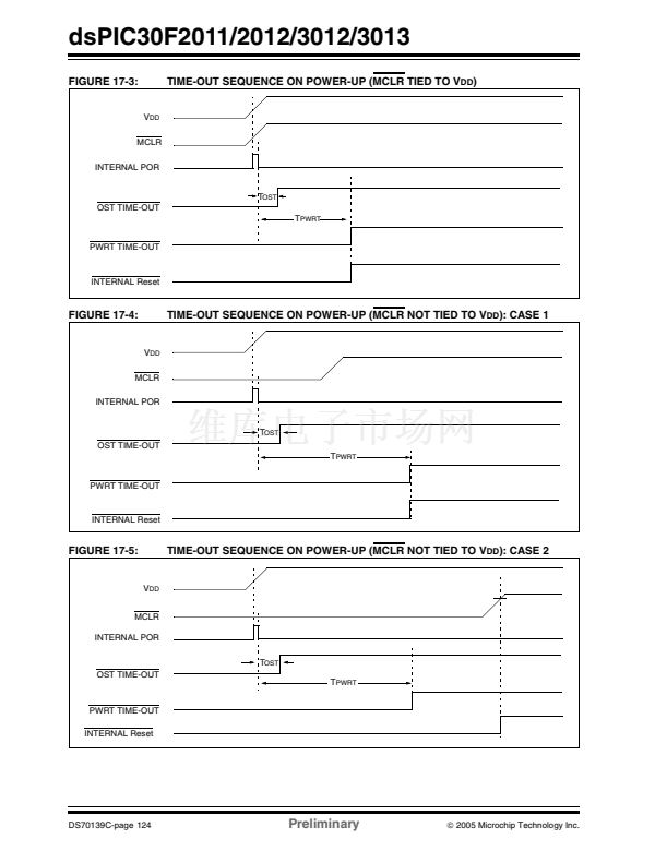
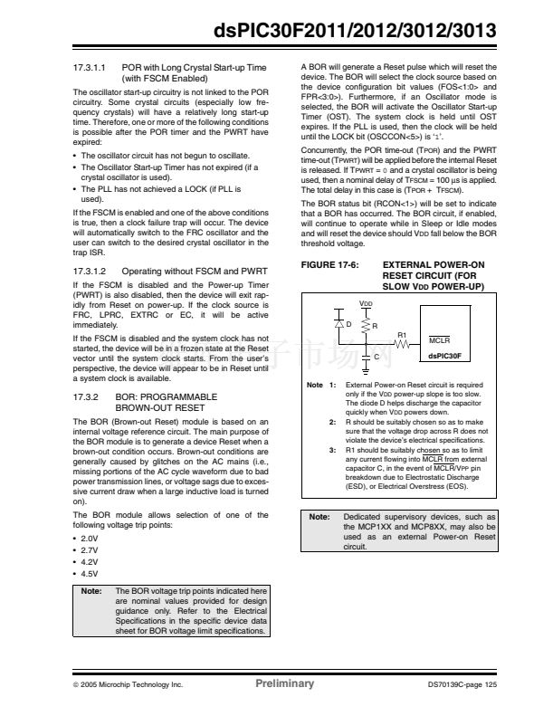
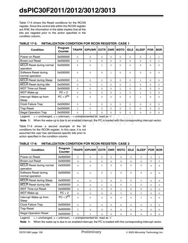
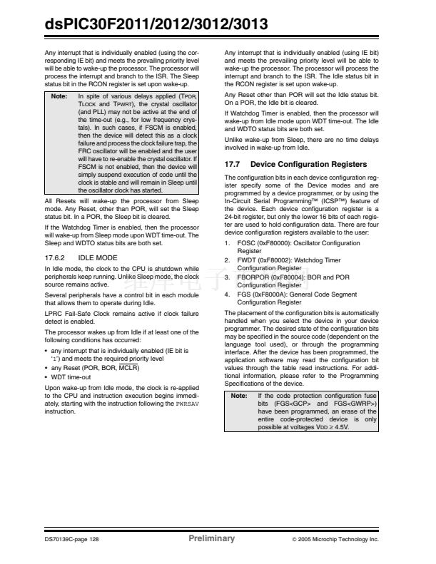
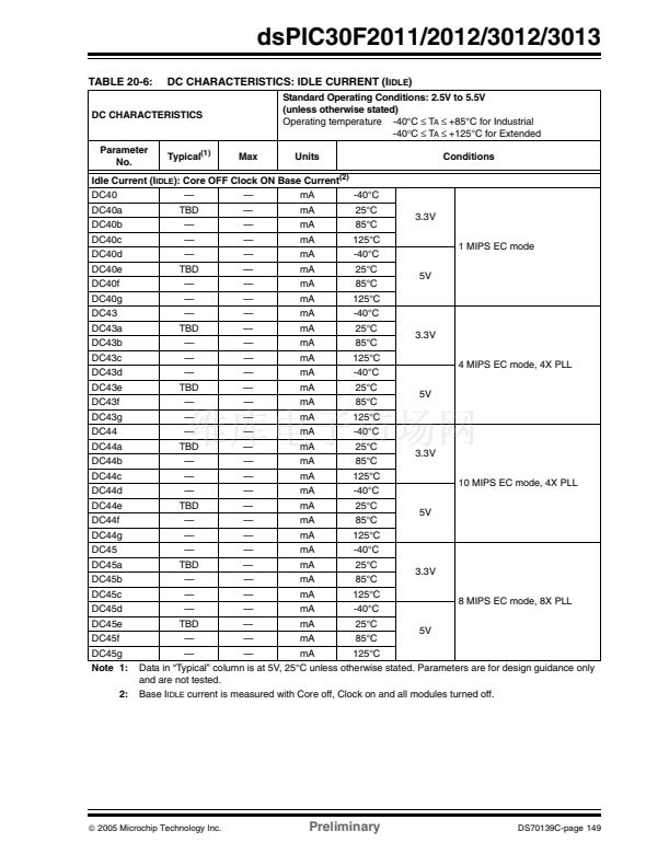
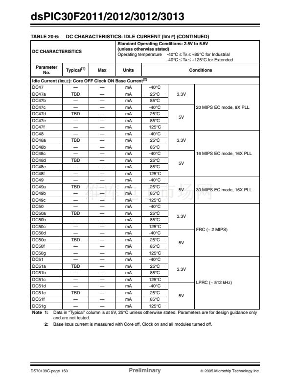
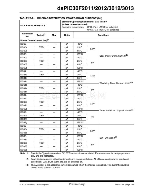
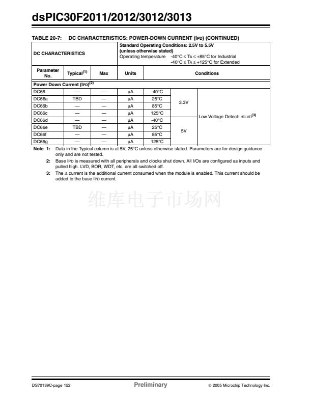
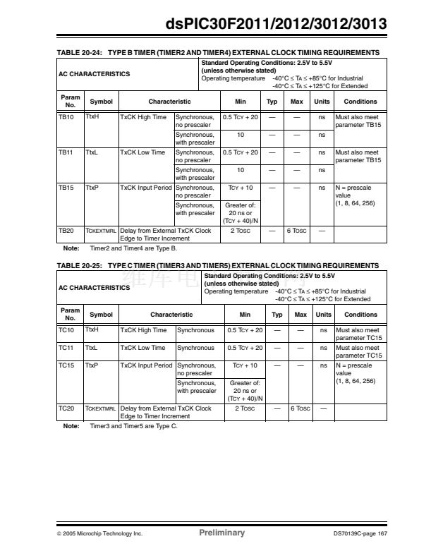
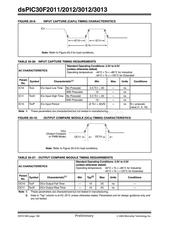
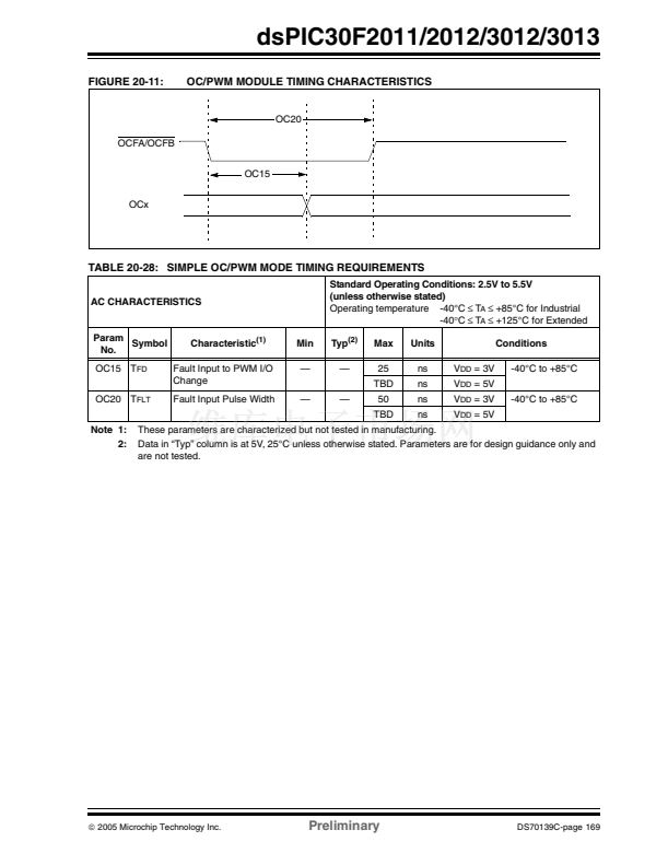
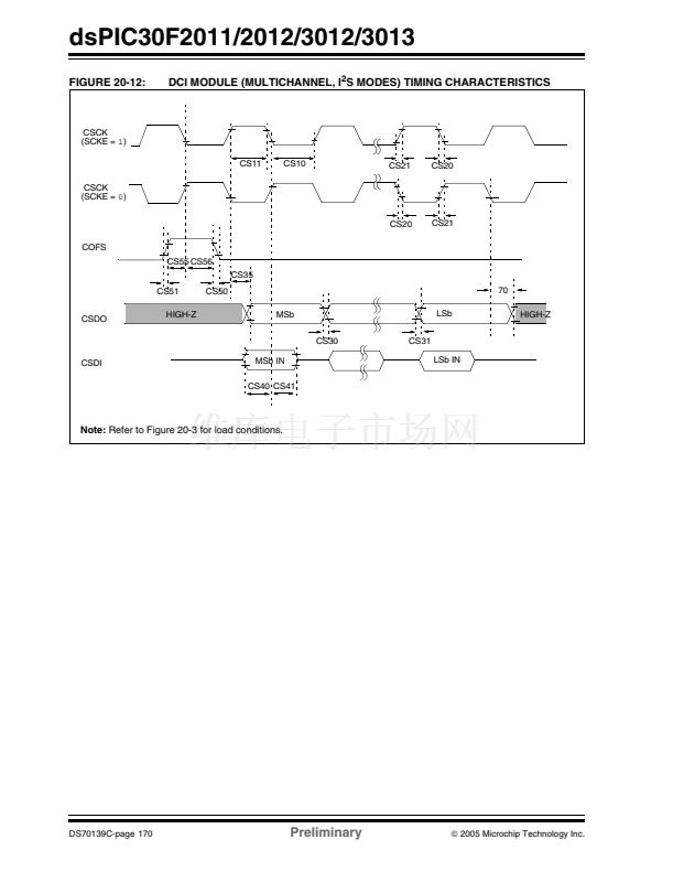
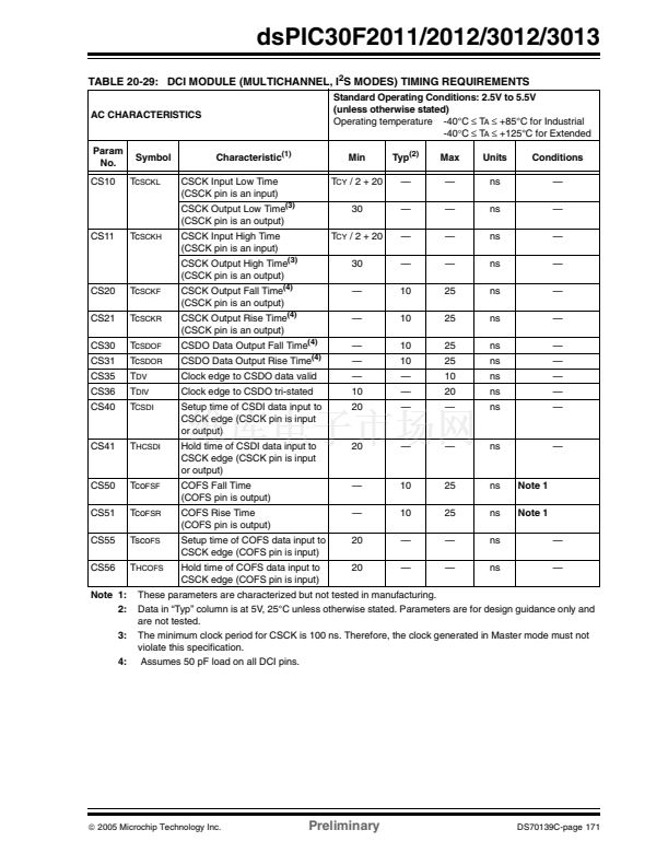
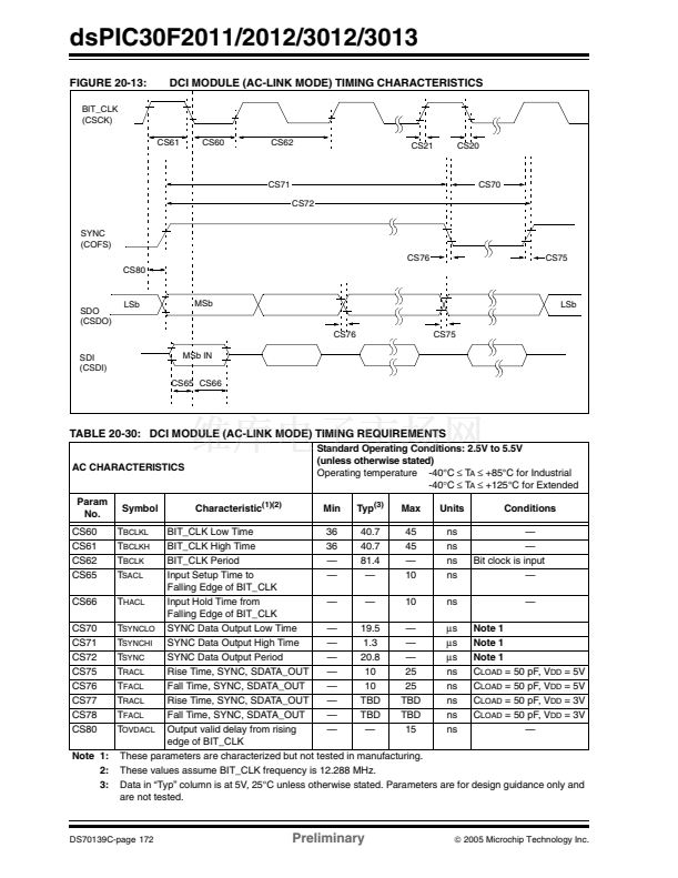
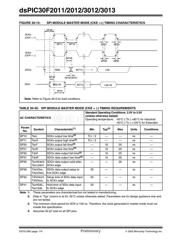
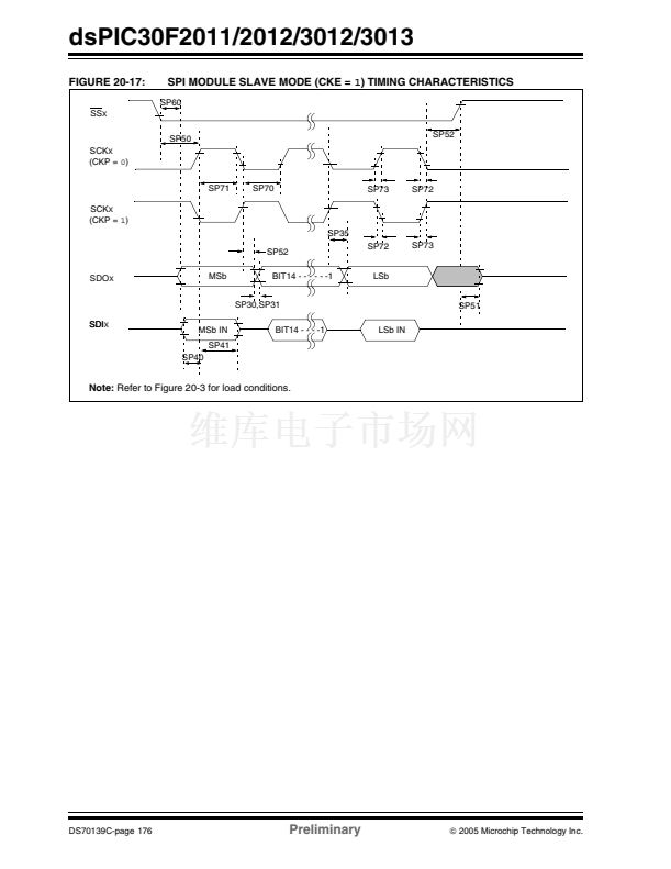
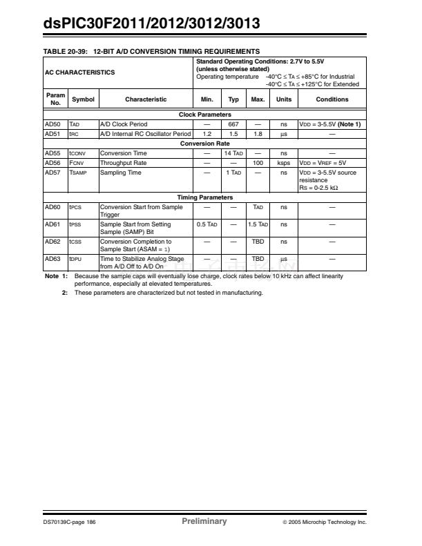
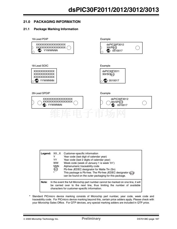
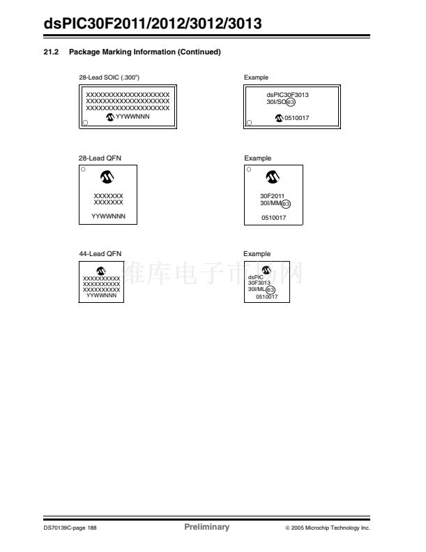
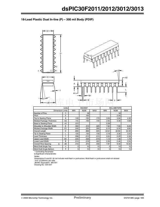
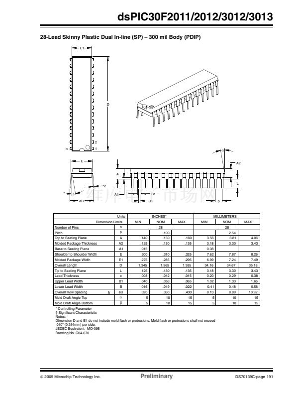
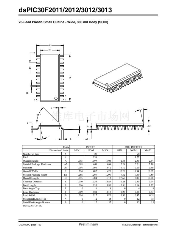
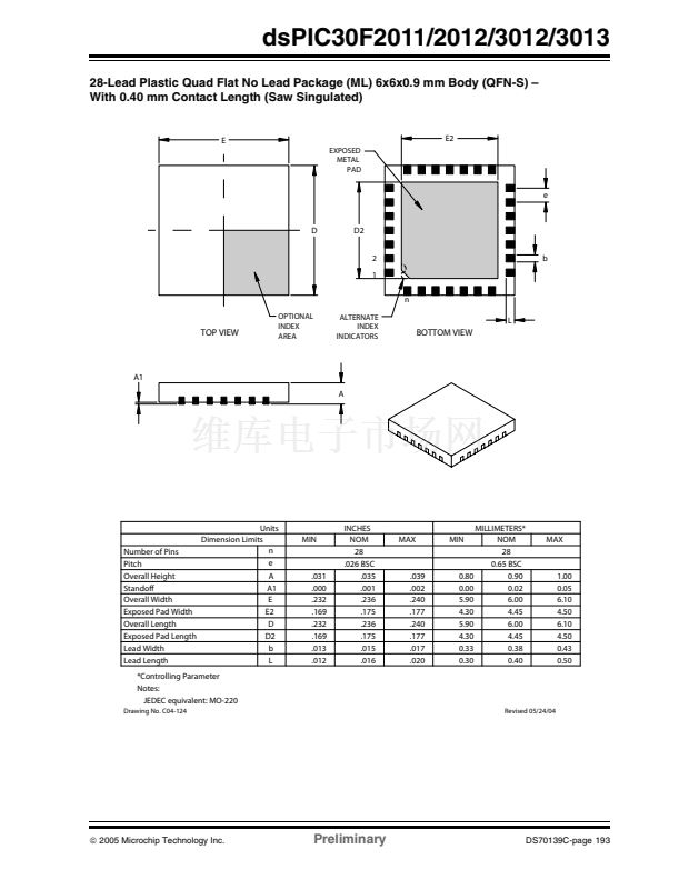
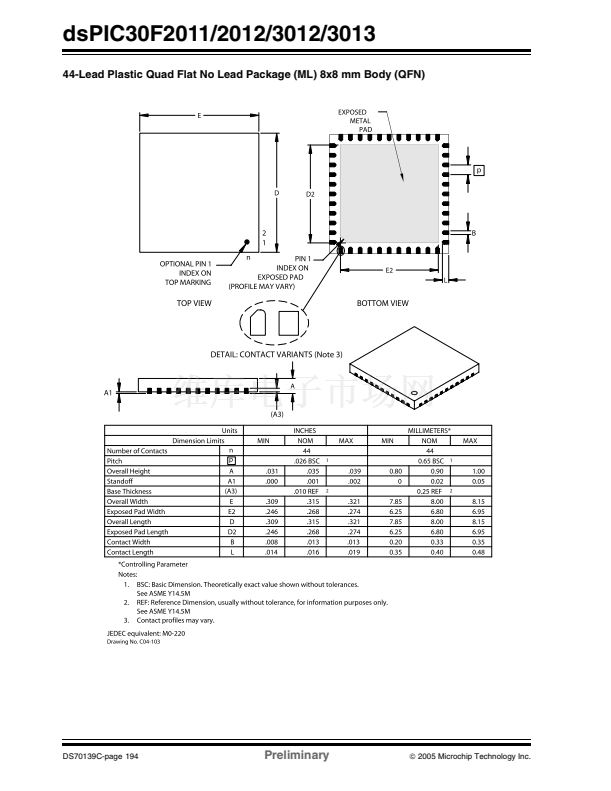
dsPIC30F2011/2012/3012/3013
5.4
RTSP Operation
5.5
Control Registers
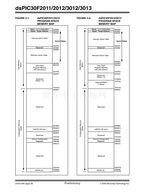
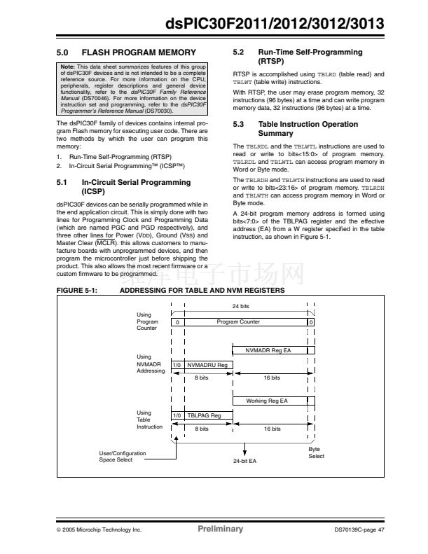
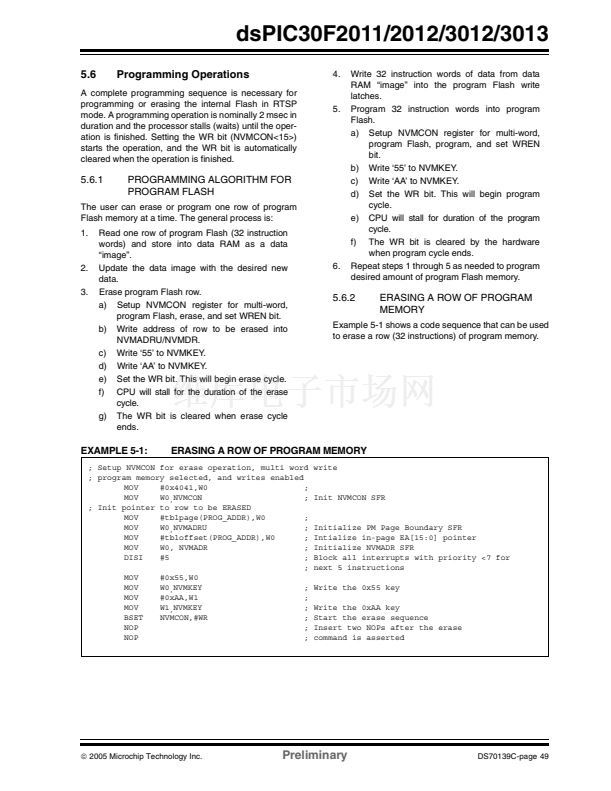
The dsPIC30F Flash program memory is organized
into rows and panels. Each row consists of 32 instruc-
tions, or 96 bytes. Each panel consists of 128 rows, or
4K x 24 instructions. RTSP allows the user to erase one
row (32 instructions) at a time and to program four
instructions at one time. RTSP may be used to program
multiple program memory panels, but the table pointer
must be changed at each panel boundary.
Each panel of program memory contains write latches
that hold 32 instructions of programming data. Prior to
the actual programming operation, the write data must
be loaded into the panel write latches. The data to be
programmed into the panel is loaded in sequential
order into the write latches; instruction
0,
instruction
1,
etc. The instruction words loaded must always be from
a group of 32 boundary.
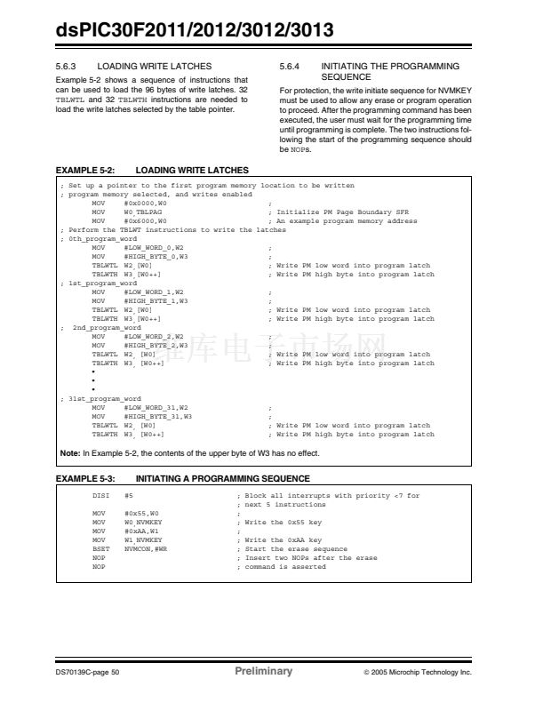
The basic sequence for RTSP programming is to set up
a table pointer, then do a series of
TBLWT
instructions
to load the write latches. Programming is performed by
setting the special bits in the NVMCON register. 32
TBLWTL
and four
TBLWTH
instructions are required to
load the 32 instructions. If multiple panel programming
is required, the table pointer needs to be changed and
the next set of multiple write latches written.
All of the table write operations are single word writes
(2 instruction cycles), because only the table latches
are written. A programming cycle is required for
programming each row.
The Flash Program Memory is readable, writable and
erasable during normal operation over the entire V
DD
range.
The four SFRs used to read and write the program
Flash memory are:
鈥?/div>
鈥?/div>
鈥?/div>
鈥?/div>
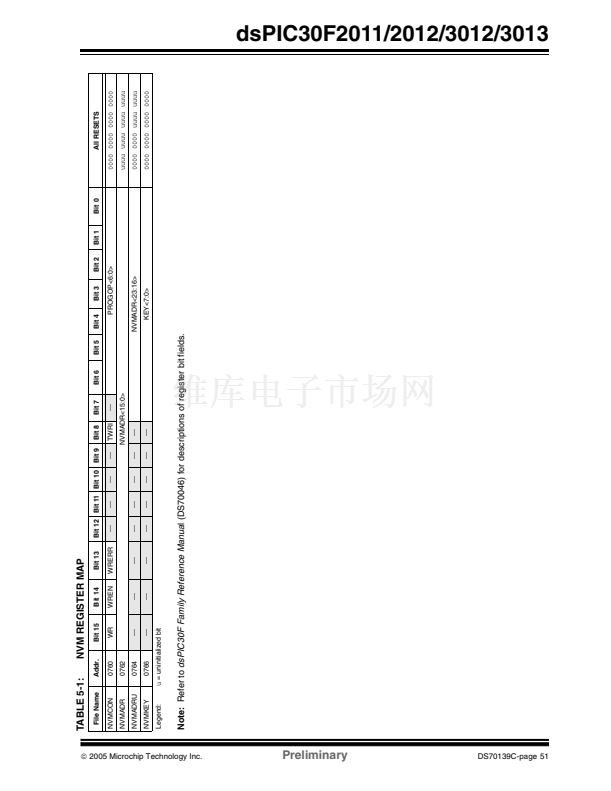
NVMCON
NVMADR
NVMADRU
NVMKEY
5.5.1
NVMCON REGISTER
The NVMCON register controls which blocks are to be
erased, which memory type is to be programmed, and
start of the programming cycle.
5.5.2
NVMADR REGISTER
The NVMADR register is used to hold the lower two
bytes of the effective address. The NVMADR register
captures the EA<15:0> of the last table instruction that
has been executed and selects the row to write.
5.5.3
NVMADRU REGISTER
The NVMADRU register is used to hold the upper byte
of the effective address. The NVMADRU register cap-
tures the EA<23:16> of the last table instruction that
has been executed.
5.5.4
NVMKEY REGISTER
NVMKEY is a write-only register that is used for write
protection. To start a programming or an erase
sequence, the user must consecutively write 0x55 and
0xAA to the NVMKEY register. Refer to Section 5.6 for
further details.
Note:
The user can also directly write to the
NVMADR and NVMADRU registers to
specify a program memory address for
erasing or programming.
DS70139C-page 48
Preliminary
漏
2005 Microchip Technology Inc.


 1
1
 2
2
 3
3
 4
4
 5
5
 6
6
 7
7
 8
8
 9
9
 10
10
 11
11
 12
12
 13
13
 14
14
 15
15
 16
16
 17
17
 18
18
 19
19
 20
20
 21
21
 22
22
 23
23
 24
24
 25
25
 26
26
 27
27
 28
28
 29
29
 30
30
 31
31
 32
32
 33
33
 34
34
 35
35
 36
36
 37
37
 38
38
 39
39
 40
40
 41
41
 42
42
 43
43
 44
44
 45
45
 46
46
 47
47
 48
48
 49
49
 50
50
 51
51
 52
52
 53
53
 54
54
 55
55
 56
56
 57
57
 58
58
 59
59
 60
60
 61
61
 62
62
 63
63
 64
64
 65
65
 66
66
 67
67
 68
68
 69
69
 70
70
 71
71
 72
72
 73
73
 74
74
 75
75
 76
76
 77
77
 78
78
 79
79
 80
80
 81
81
 82
82
 83
83
 84
84
 85
85
 86
86
 87
87
 88
88
 89
89
 90
90
 91
91
 92
92
 93
93
 94
94
 95
95
 96
96
 97
97
 98
98
 99
99
 100
100
 101
101
 102
102
 103
103
 104
104
 105
105
 106
106
 107
107
 108
108
 109
109
 110
110
 111
111
 112
112
 113
113
 114
114
 115
115
 116
116
 117
117
 118
118
 119
119
 120
120
 121
121
 122
122
 123
123
 124
124
 125
125
 126
126
 127
127
 128
128
 129
129
 130
130
 131
131
 132
132
 133
133
 134
134
 135
135
 136
136
 137
137
 138
138
 139
139
 140
140
 141
141
 142
142
 143
143
 144
144
 145
145
 146
146
 147
147
 148
148
 149
149
 150
150
 151
151
 152
152
 153
153
 154
154
 155
155
 156
156
 157
157
 158
158
 159
159
 160
160
 161
161
 162
162
 163
163
 164
164
 165
165
 166
166
 167
167
 168
168
 169
169
 170
170
 171
171
 172
172
 173
173
 174
174
 175
175
 176
176
 177
177
 178
178
 179
179
 180
180
 181
181
 182
182
 183
183
 184
184
 185
185
 186
186
 187
187
 188
188
 189
189
 190
190
 191
191
 192
192
 193
193
 194
194
 195
195
 196
196
 197
197
 198
198
 199
199
 200
200
 201
201
 202
202
 203
203
 204
204
 205
205
 206
206
 207
207
