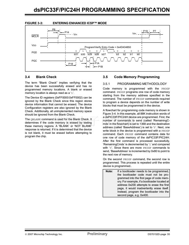
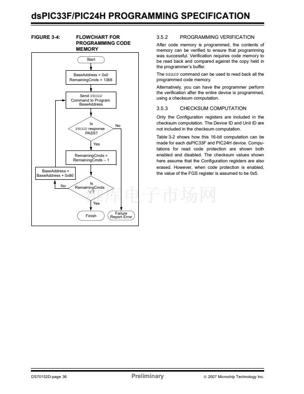
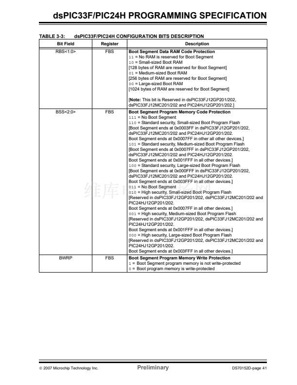
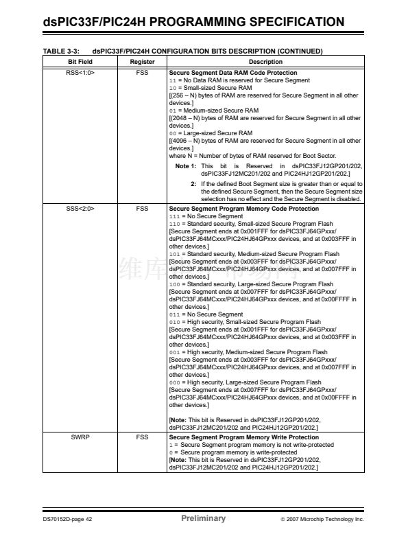
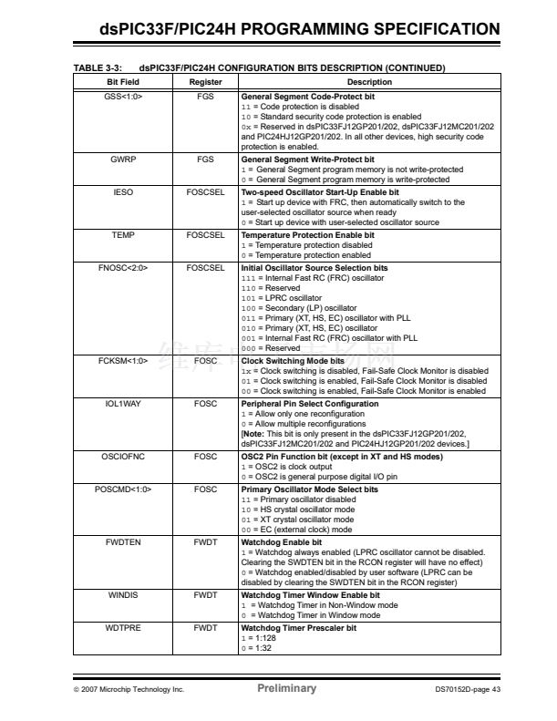
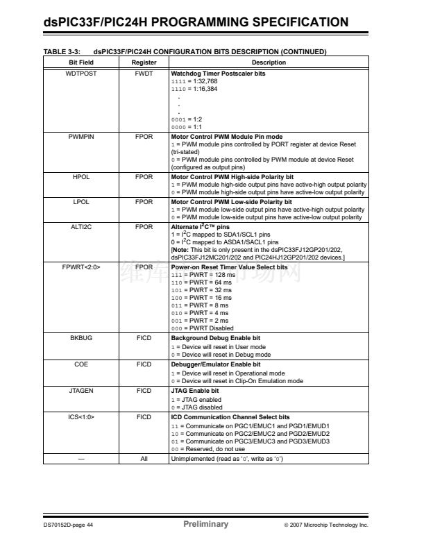
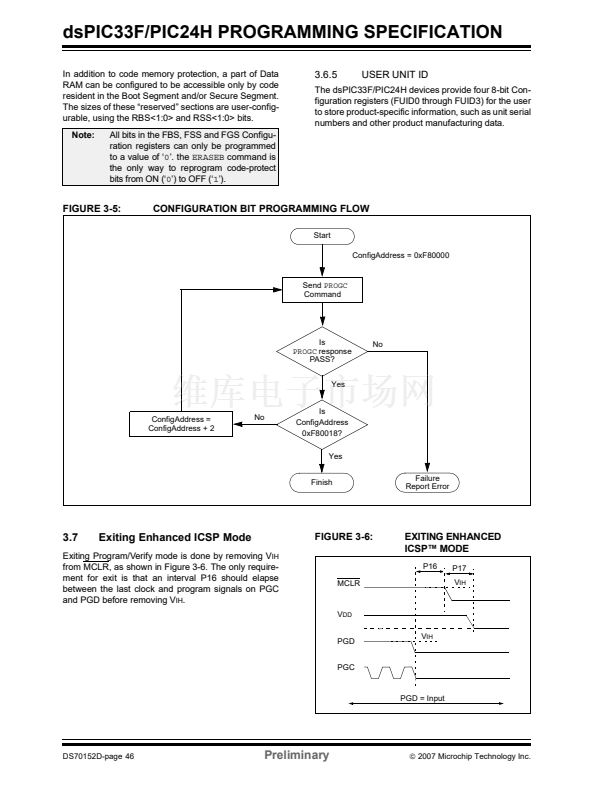
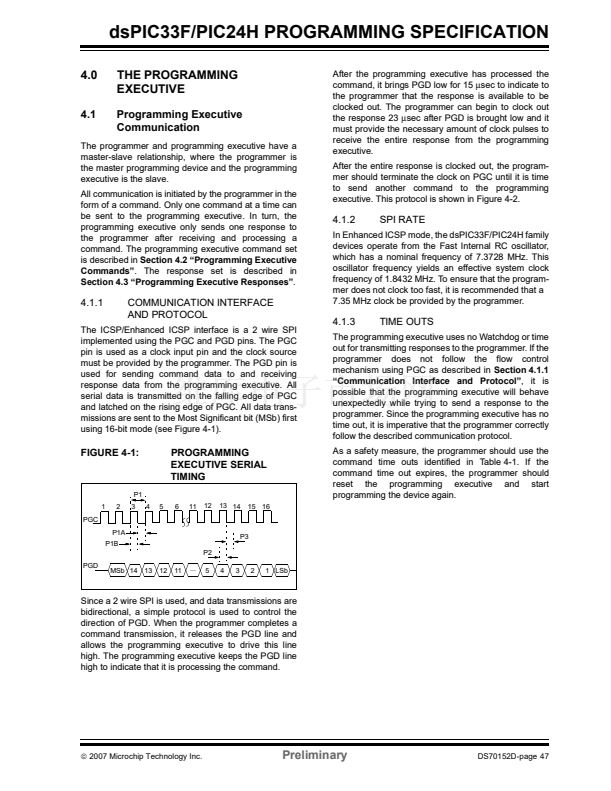
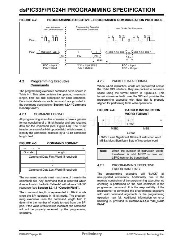
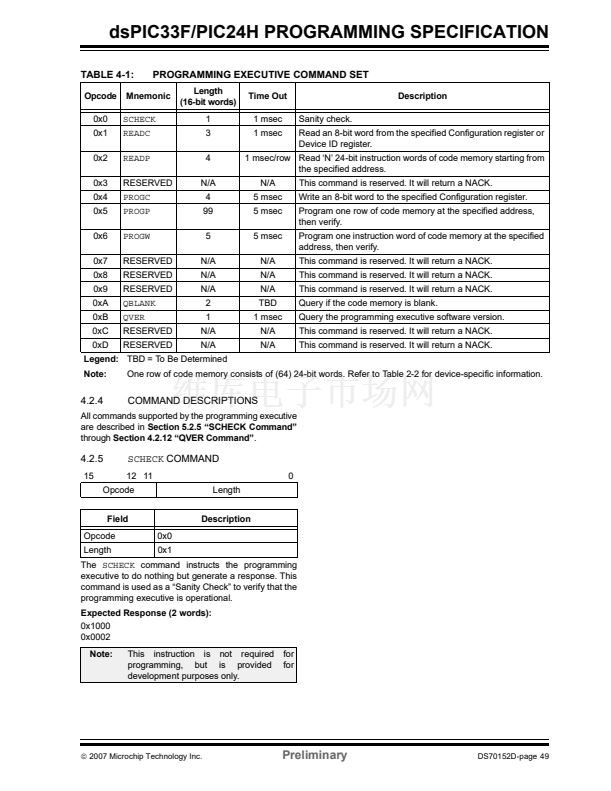
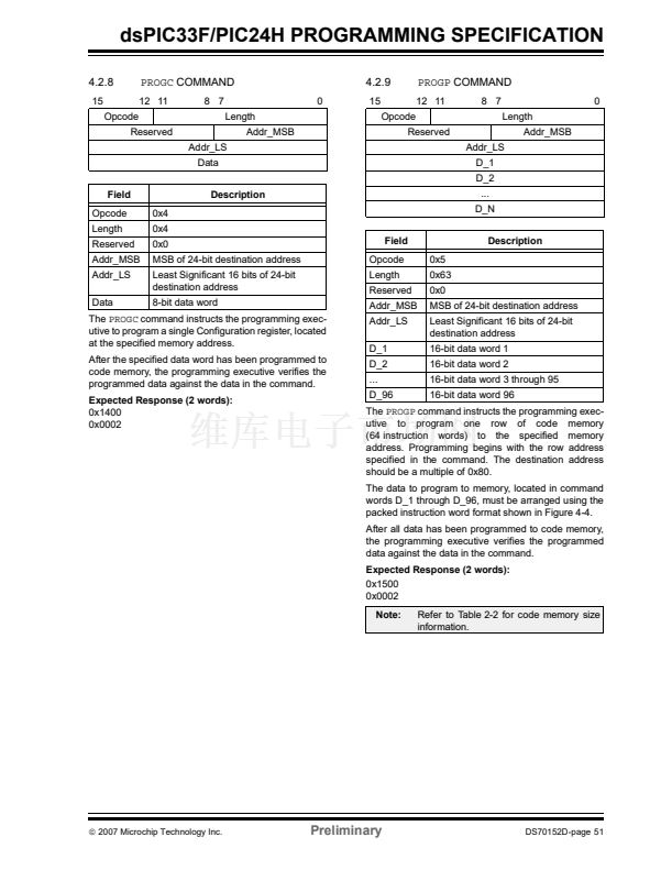
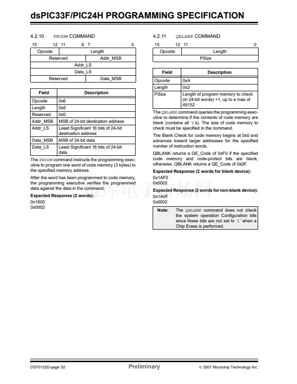
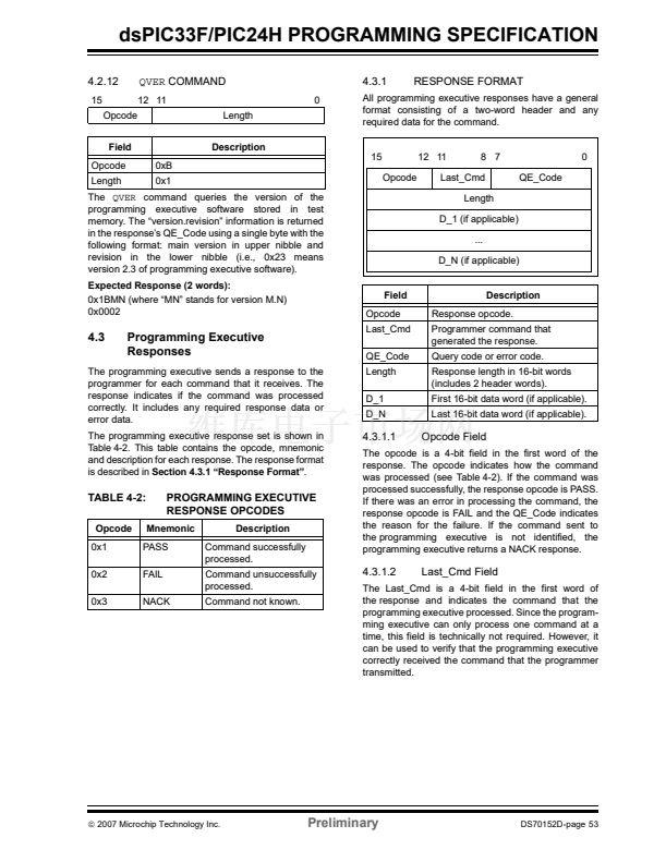
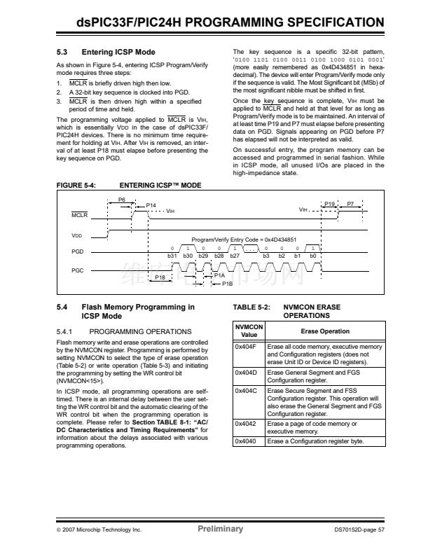
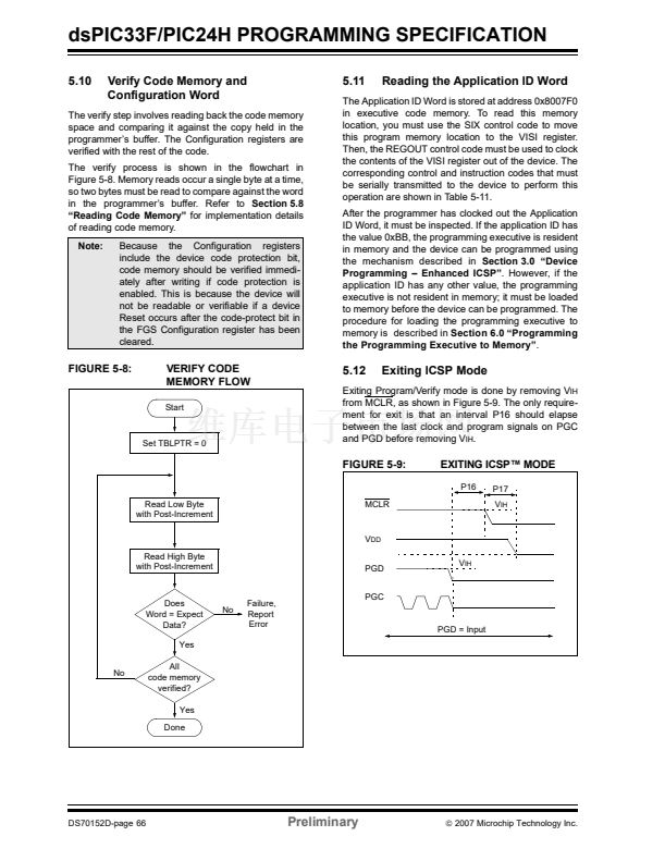
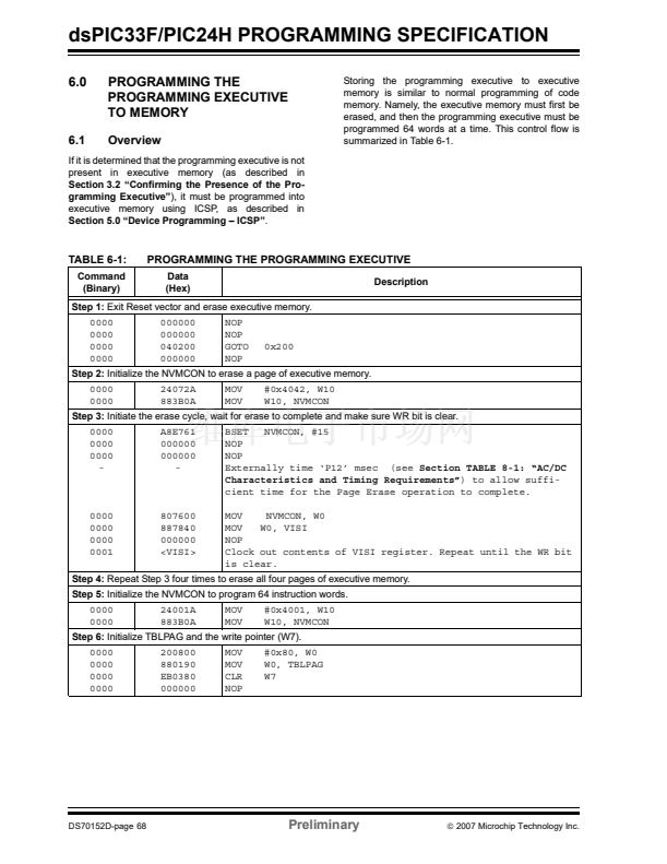
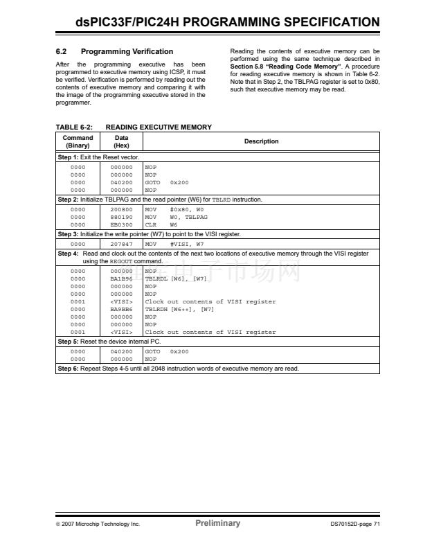
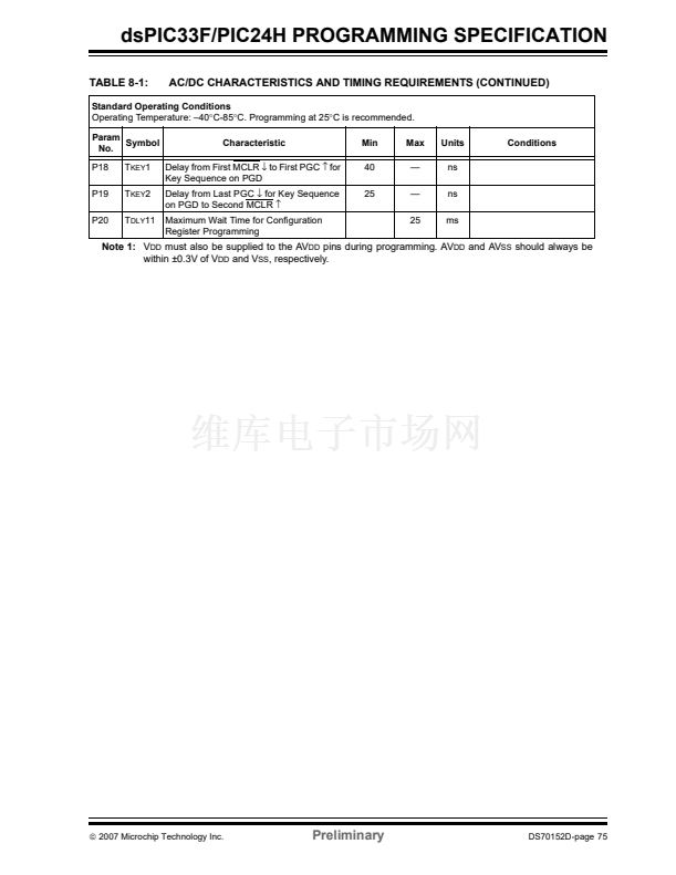
dsPIC33F/PIC24H PROGRAMMING SPECIFICATION
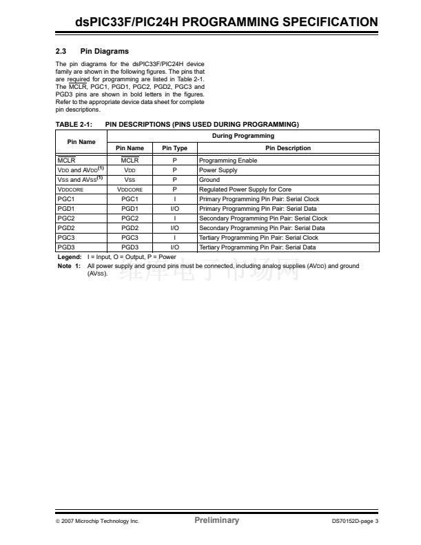
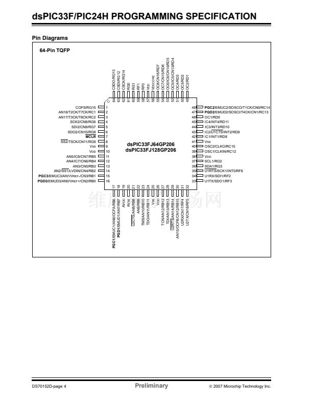
2.3
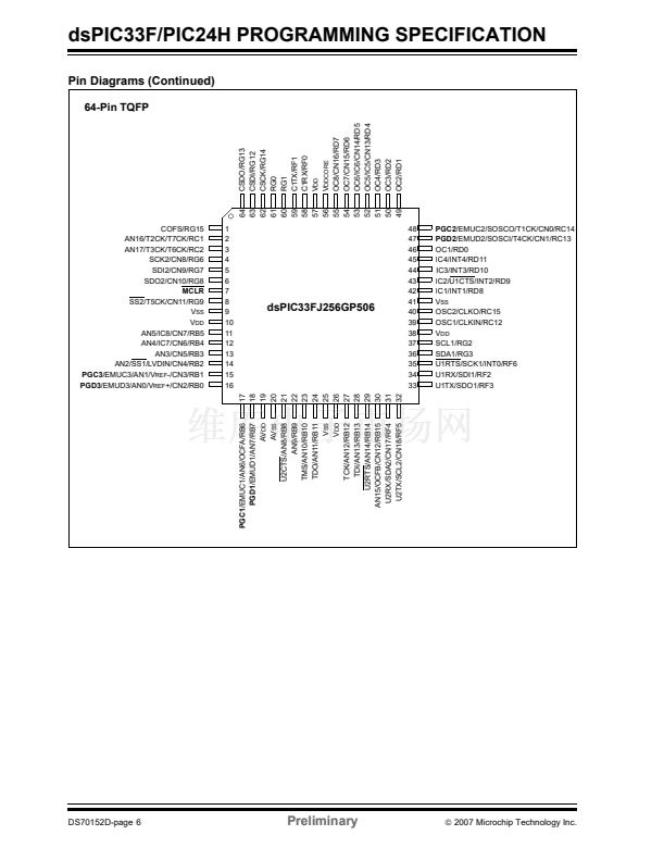
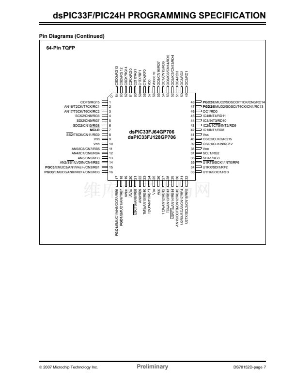
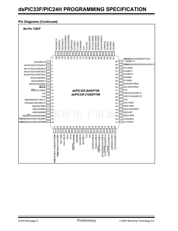
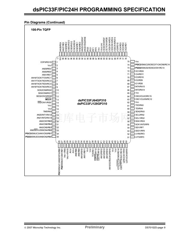
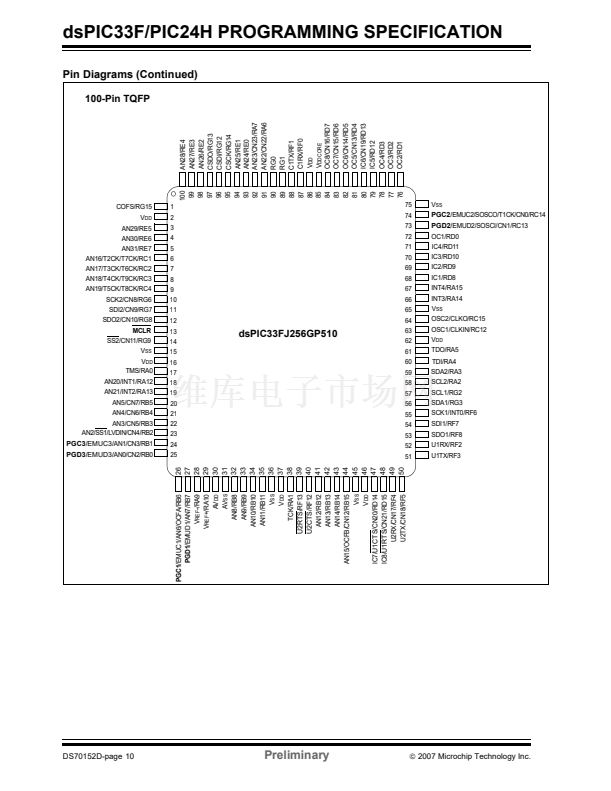
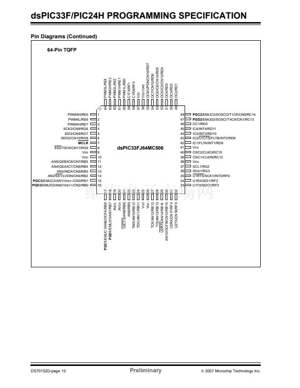
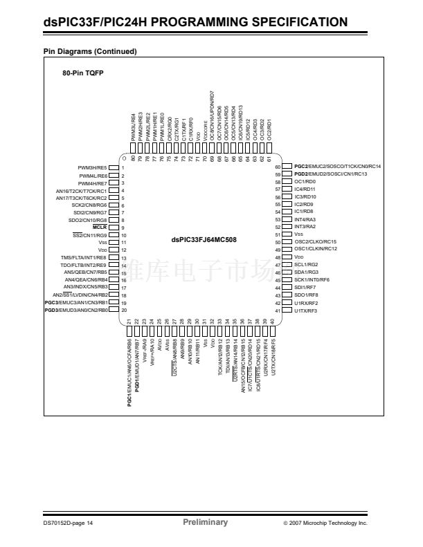
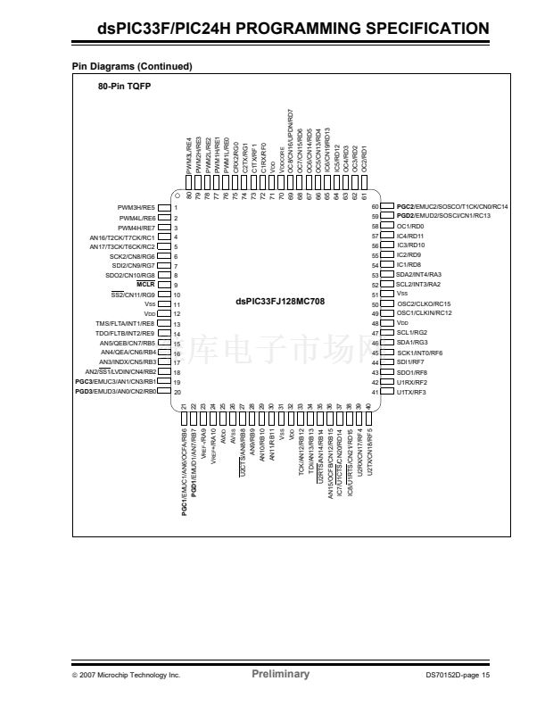
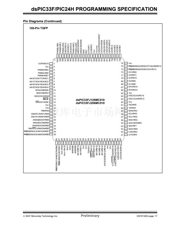
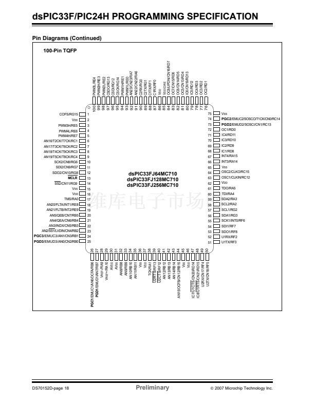
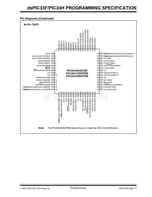
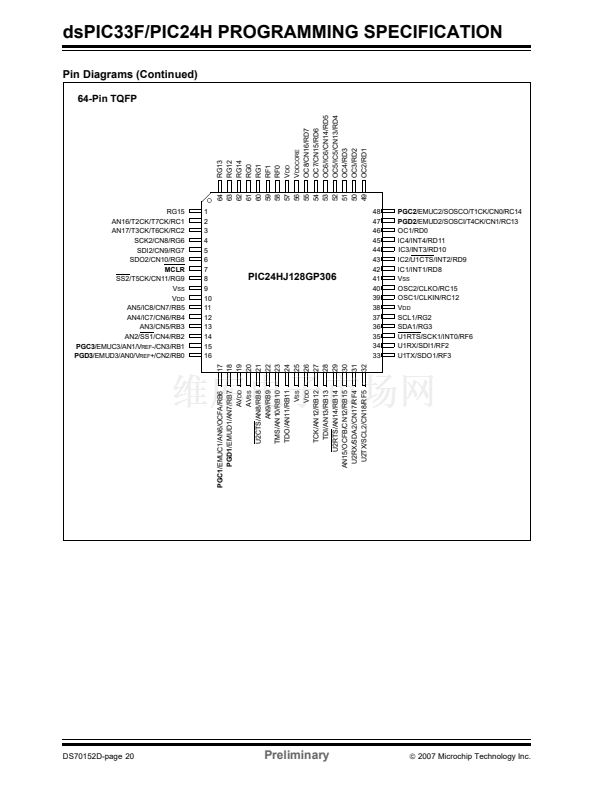
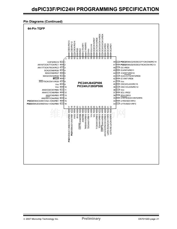
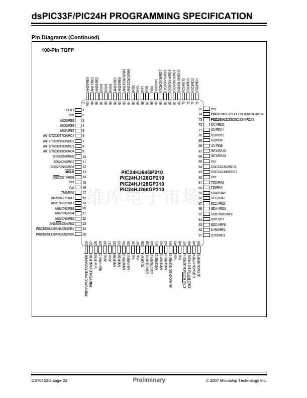
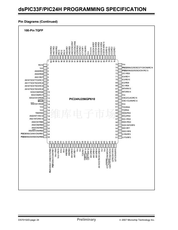
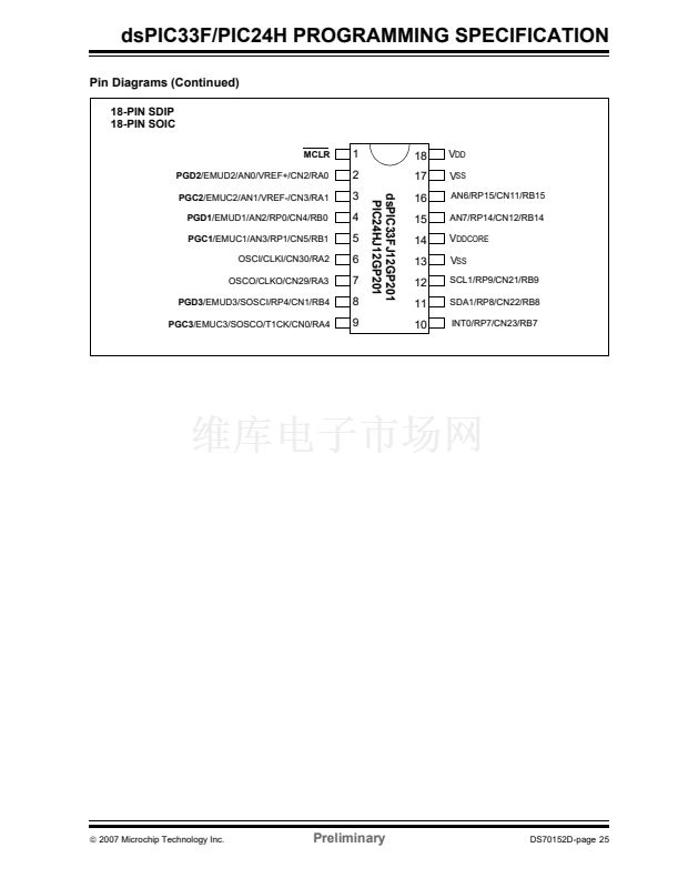
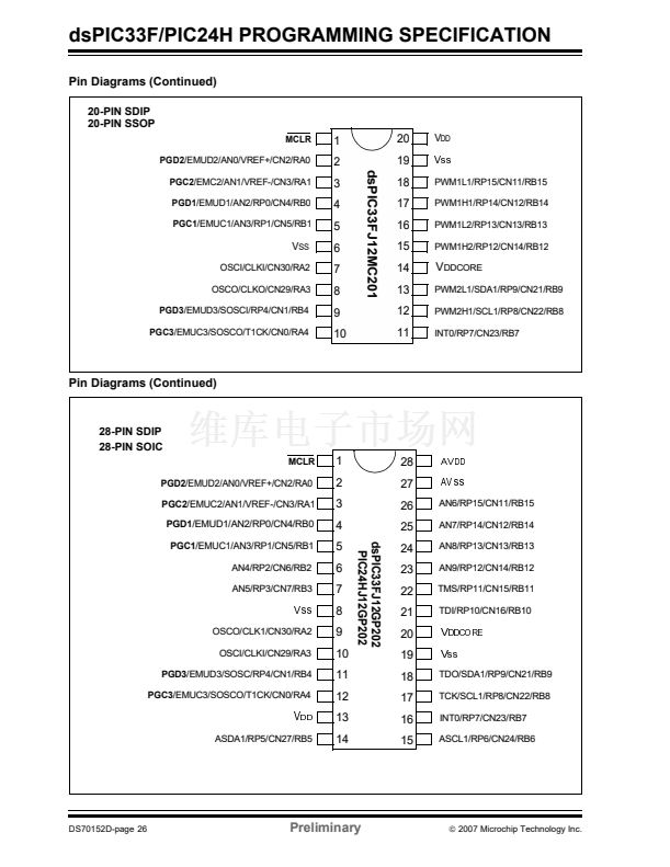
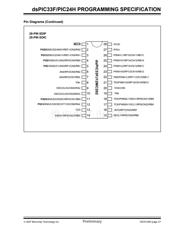
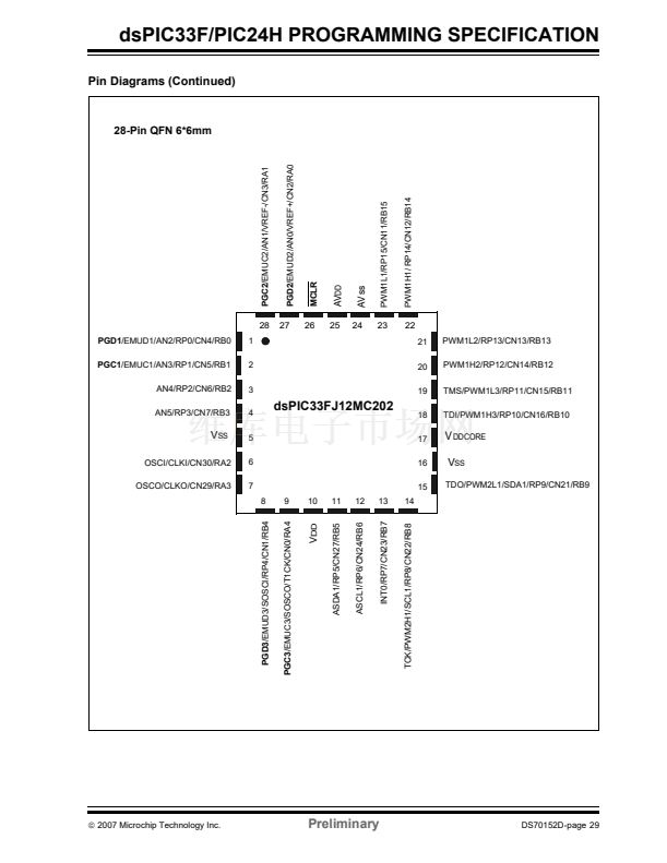
Pin Diagrams
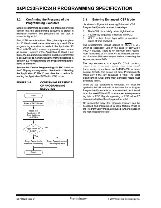
The pin diagrams for the dsPIC33F/PIC24H device
family are shown in the following figures. The pins that
are required for programming are listed in Table 2-1.
The MCLR, PGC1, PGD1, PGC2, PGD2, PGC3 and
PGD3 pins are shown in bold letters in the figures.
Refer to the appropriate device data sheet for complete
pin descriptions.
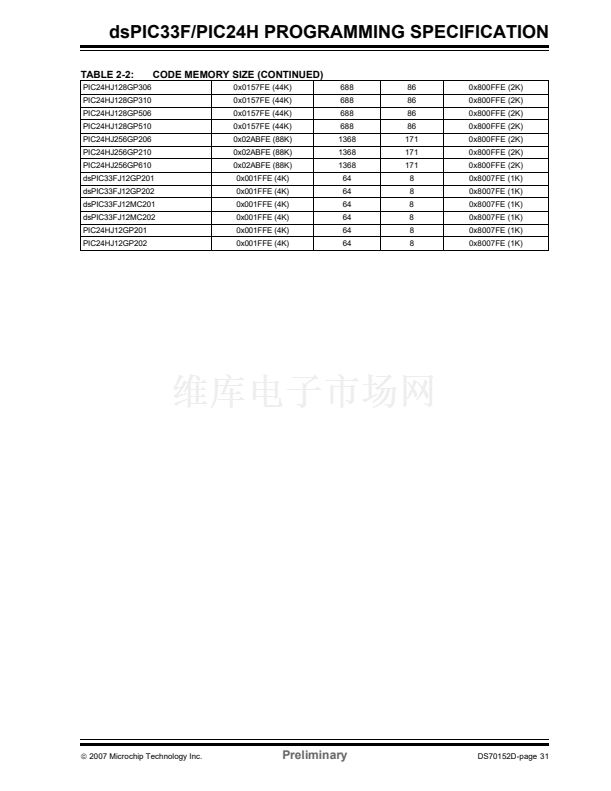
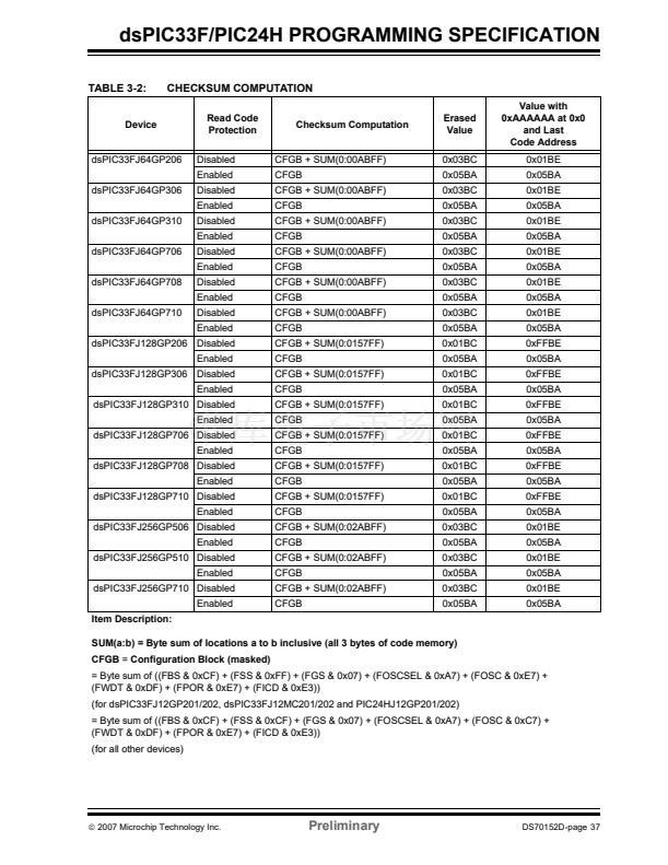
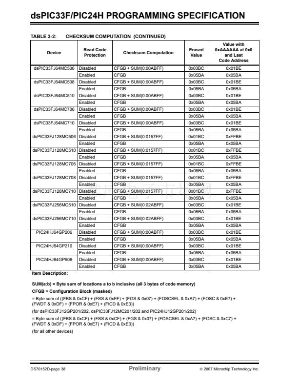
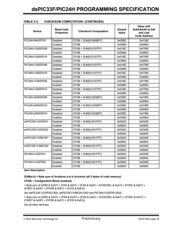
TABLE 2-1:
Pin Name
PIN DESCRIPTIONS (PINS USED DURING PROGRAMMING)
During Programming
Pin Name
Pin Type
P
P
P
P
I
I/O
I
I/O
I
I/O
Programming Enable
Power Supply
Ground
Regulated Power Supply for Core
Primary Programming Pin Pair: Serial Clock
Primary Programming Pin Pair: Serial Data
Secondary Programming Pin Pair: Serial Clock
Secondary Programming Pin Pair: Serial Data
Tertiary Programming Pin Pair: Serial Clock
Tertiary Programming Pin Pair: Serial Data
Pin Description
MCLR
V
DD
and AV
DD
(1)
V
SS
and AV
SS
(1)
V
DDCORE
PGC1
PGD1
PGC2
PGD2
PGC3
PGD3
MCLR
V
DD
V
SS
V
DDCORE
PGC1
PGD1
PGC2
PGD2
PGC3
PGD3
Legend:
I = Input, O = Output, P = Power
Note 1:
All power supply and ground pins must be connected, including analog supplies (AV
DD
) and ground
(AV
SS
).
漏
2007 Microchip Technology Inc.
Preliminary
DS70152D-page 3


 1
1
 2
2
 3
3
 4
4
 5
5
 6
6
 7
7
 8
8
 9
9
 10
10
 11
11
 12
12
 13
13
 14
14
 15
15
 16
16
 17
17
 18
18
 19
19
 20
20
 21
21
 22
22
 23
23
 24
24
 25
25
 26
26
 27
27
 28
28
 29
29
 30
30
 31
31
 32
32
 33
33
 34
34
 35
35
 36
36
 37
37
 38
38
 39
39
 40
40
 41
41
 42
42
 43
43
 44
44
 45
45
 46
46
 47
47
 48
48
 49
49
 50
50
 51
51
 52
52
 53
53
 54
54
 55
55
 56
56
 57
57
 58
58
 59
59
 60
60
 61
61
 62
62
 63
63
 64
64
 65
65
 66
66
 67
67
 68
68
 69
69
 70
70
 71
71
 72
72
 73
73
 74
74
 75
75
 76
76
 77
77
 78
78
 79
79
 80
80
