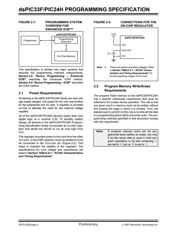
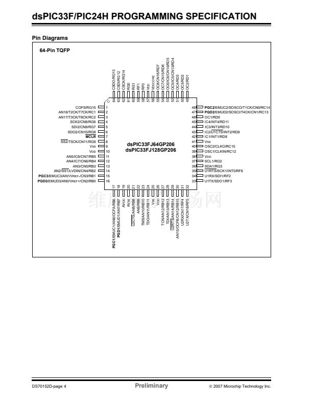
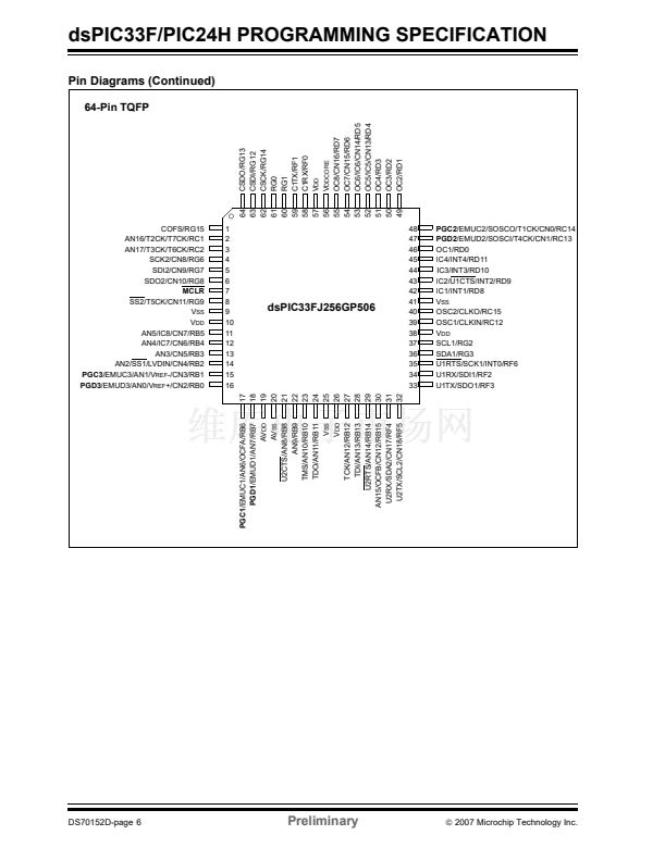
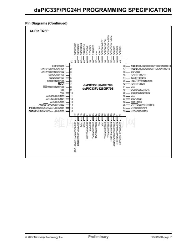
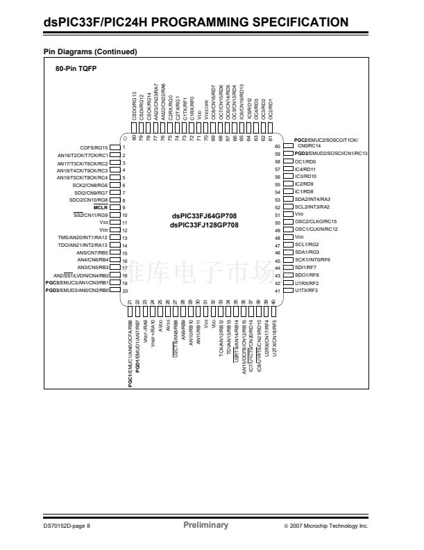
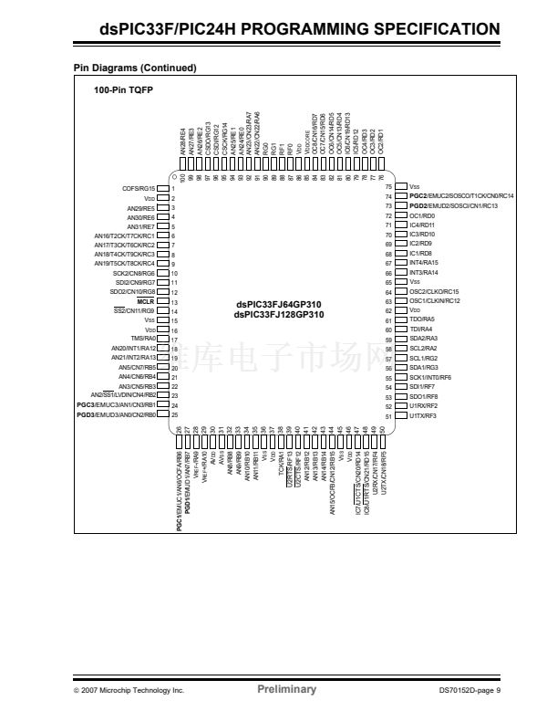
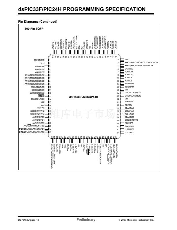
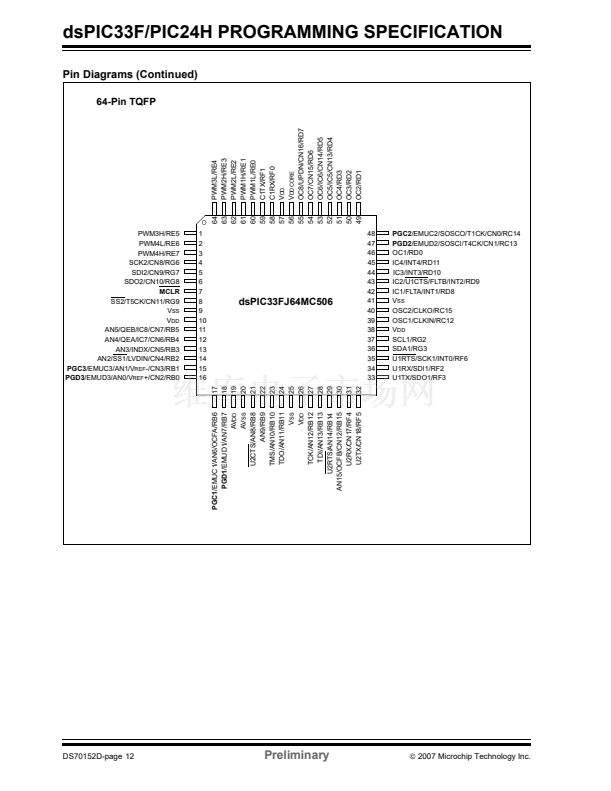
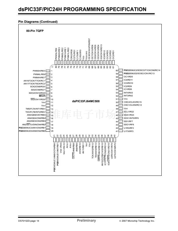
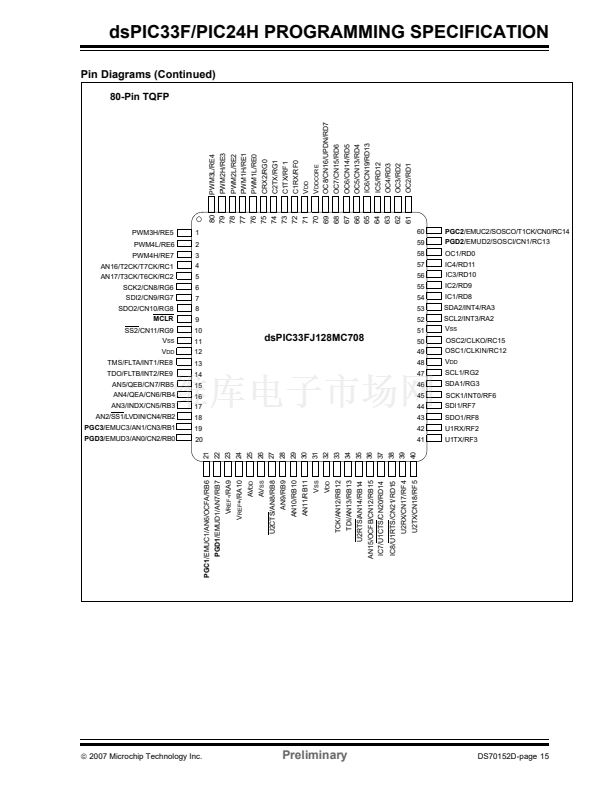
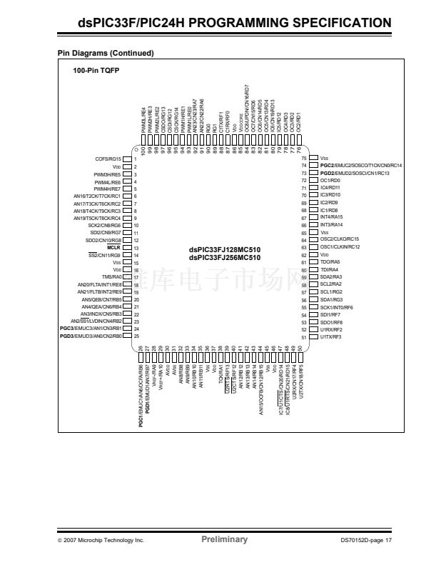
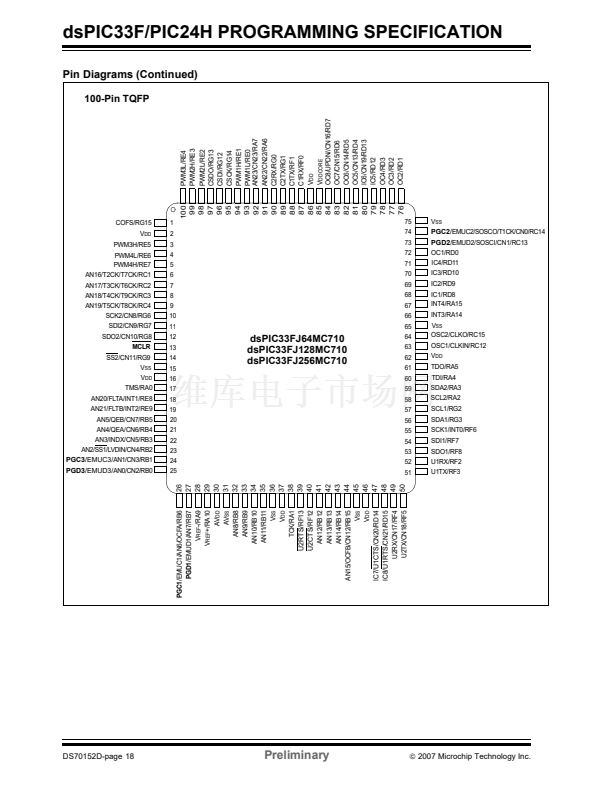
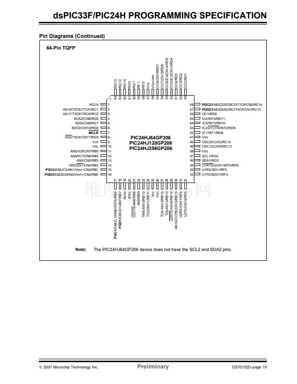
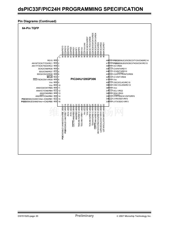
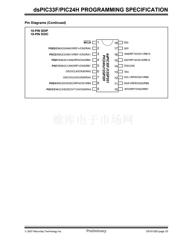
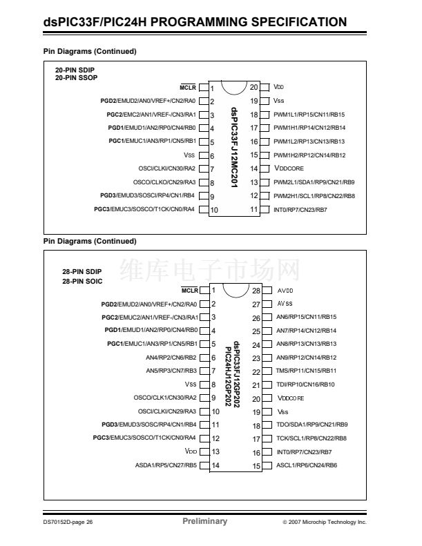
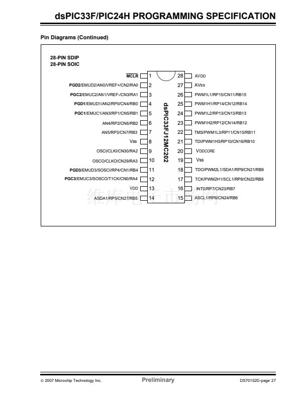
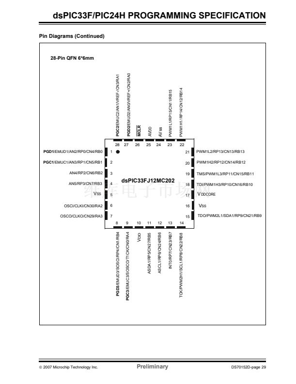
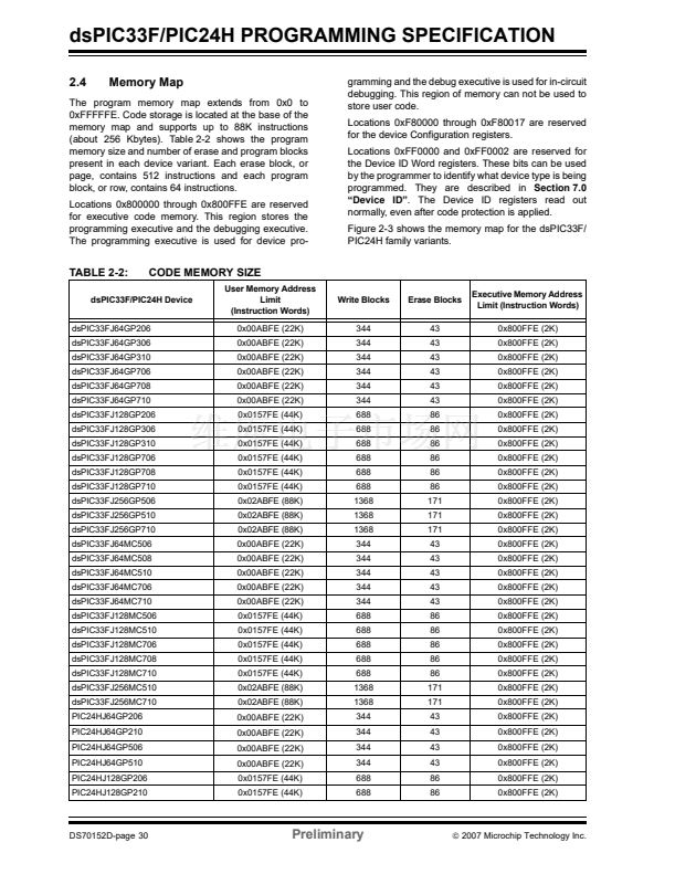
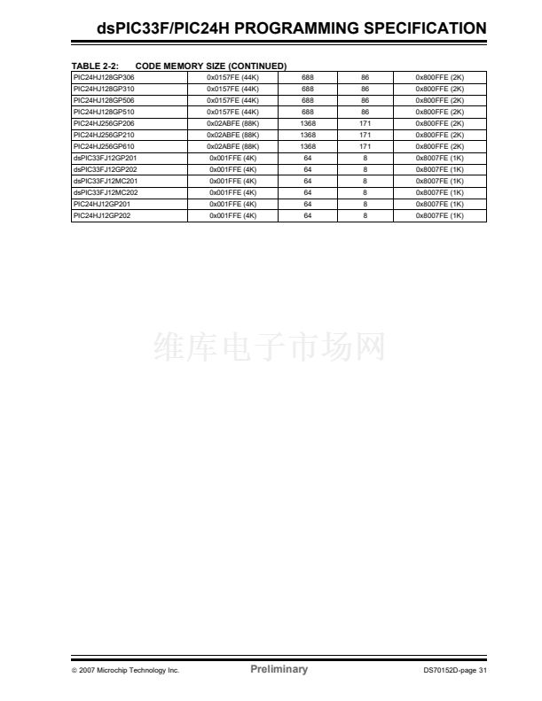
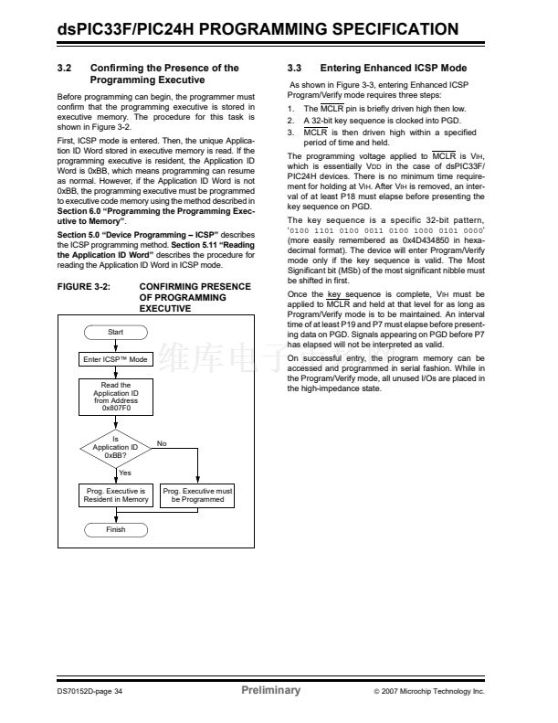
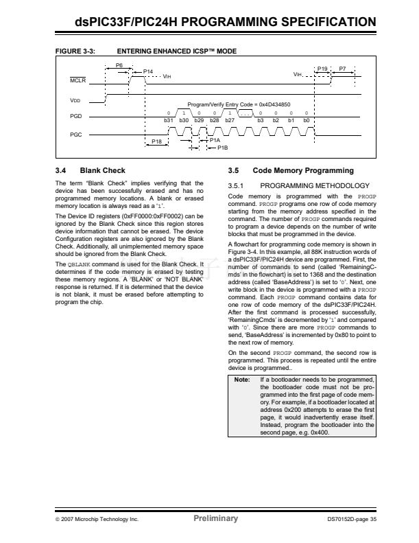
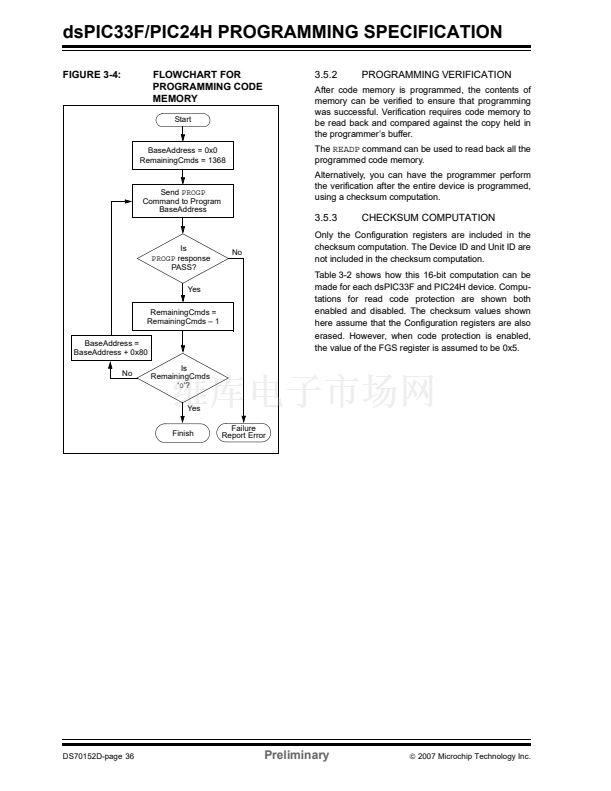
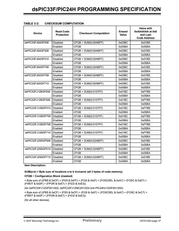
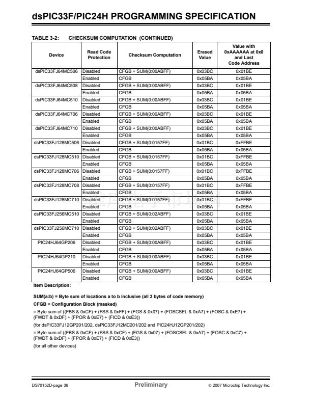
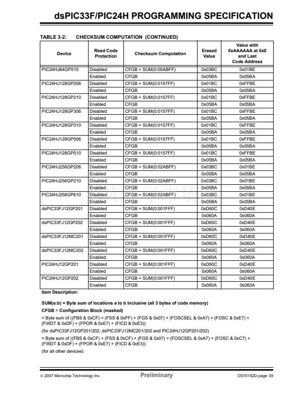
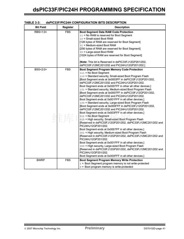
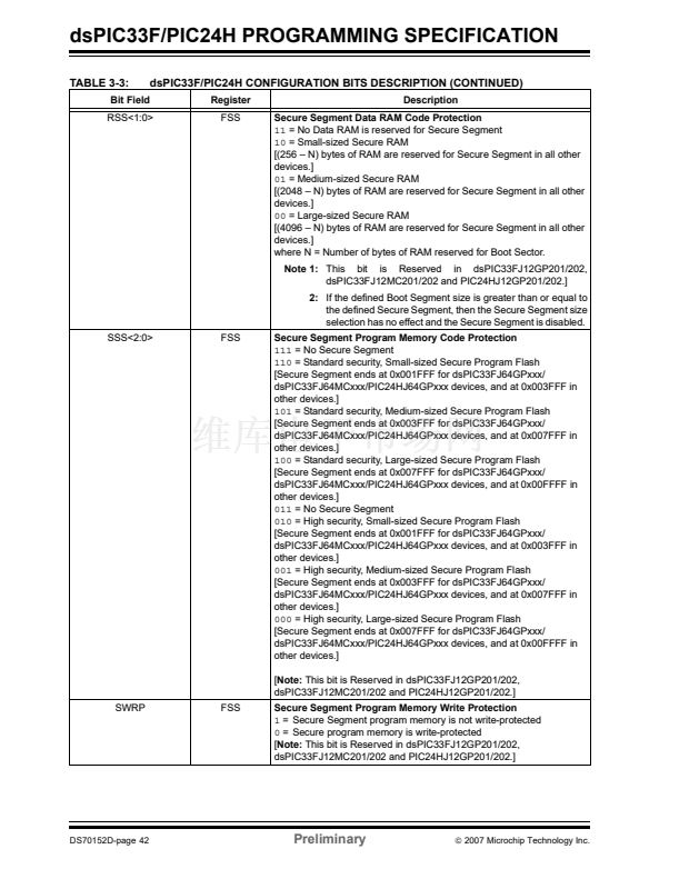
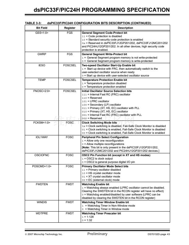
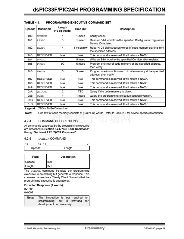
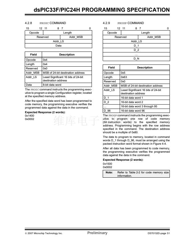
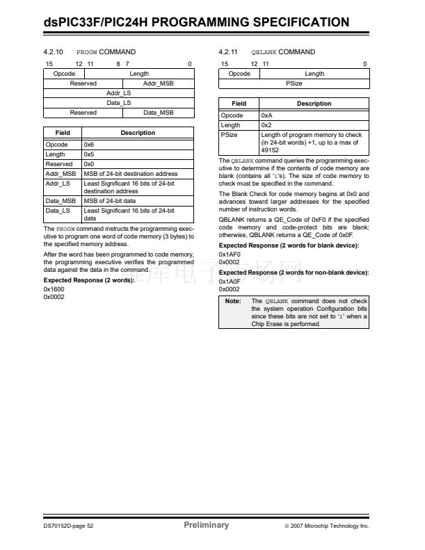
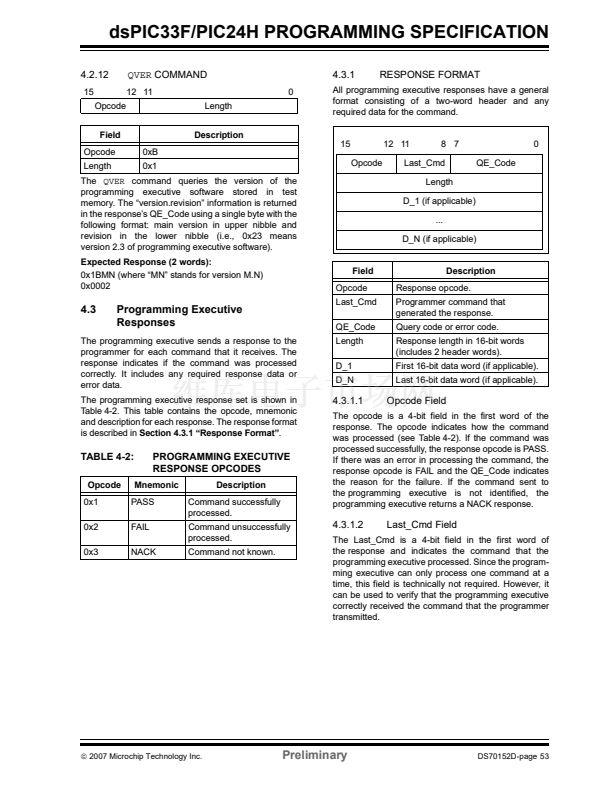
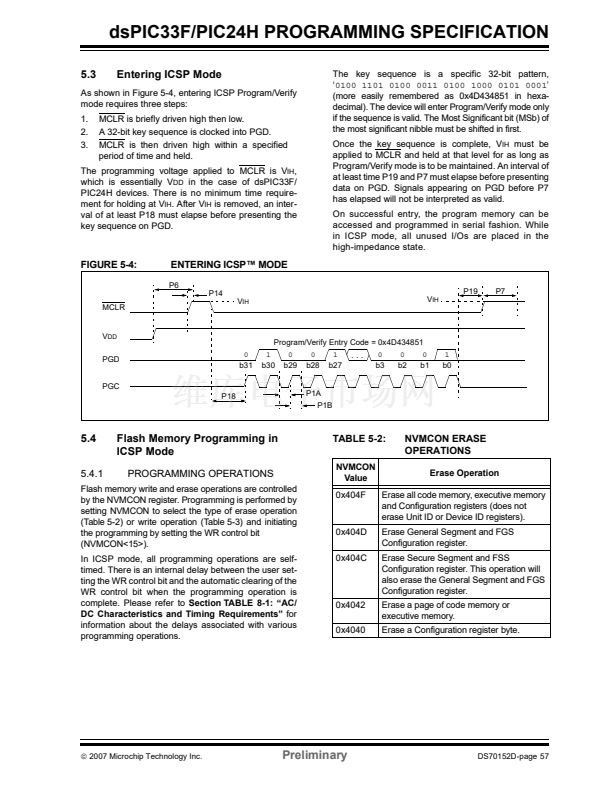
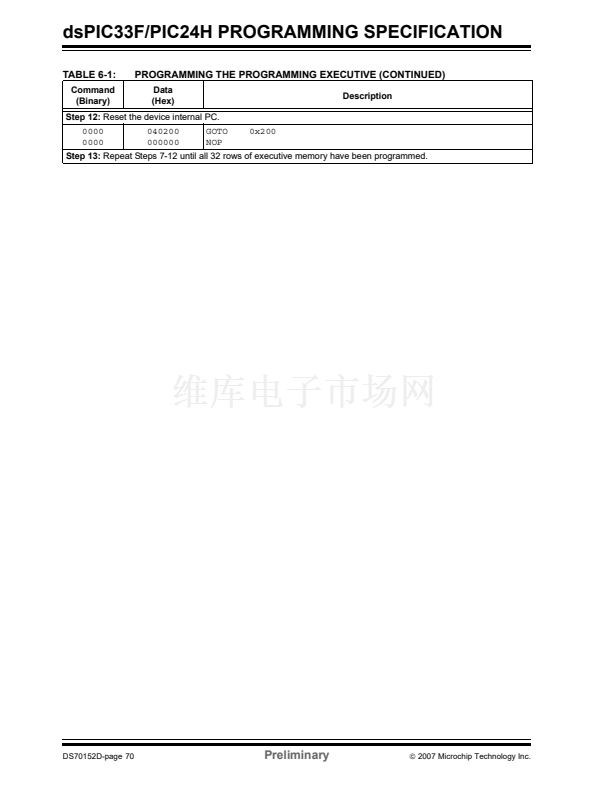
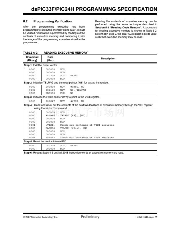
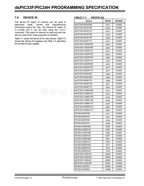
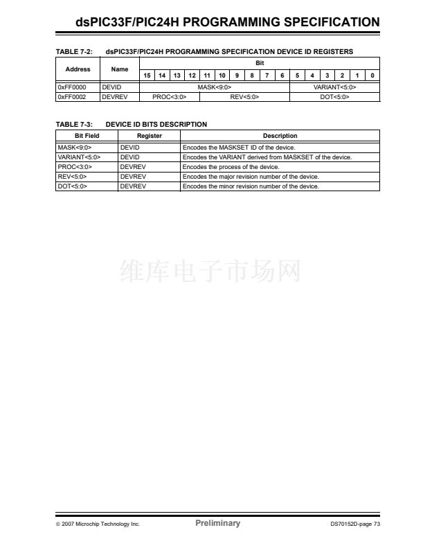
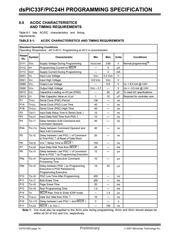
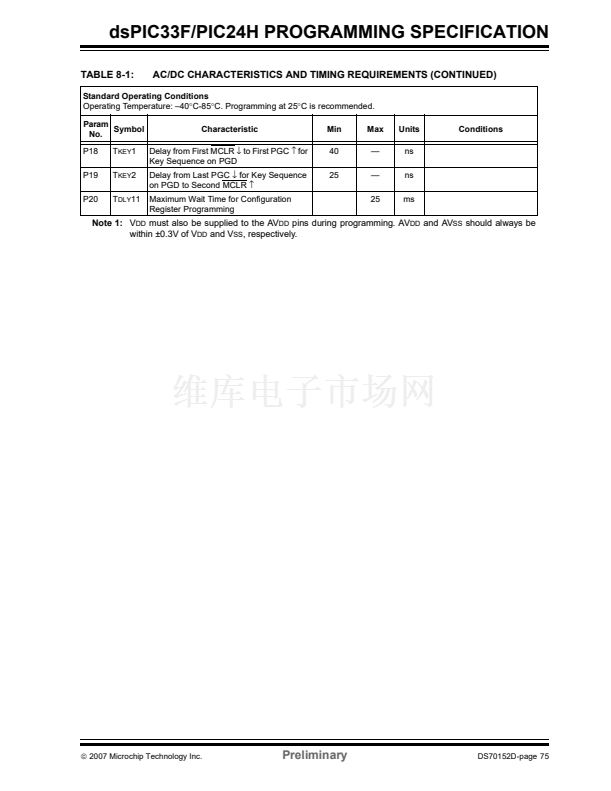
dsPIC33F/PIC24H PROGRAMMING SPECIFICATION
4.0
4.1
THE PROGRAMMING
EXECUTIVE
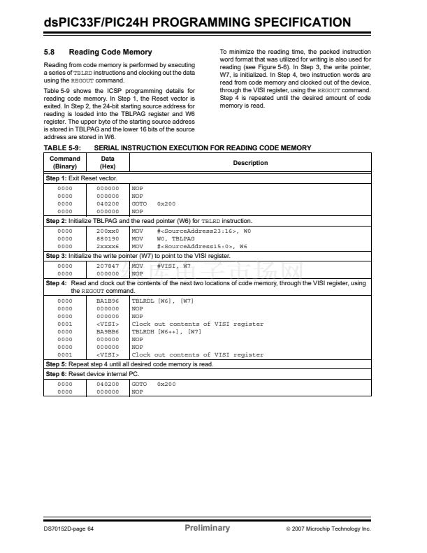
Programming Executive
Communication
The programmer and programming executive have a
master-slave relationship, where the programmer is
the master programming device and the programming
executive is the slave.
All communication is initiated by the programmer in the
form of a command. Only one command at a time can
be sent to the programming executive. In turn, the
programming executive only sends one response to
the programmer after receiving and processing a
command. The programming executive command set
is described in
Section 4.2 鈥淧rogramming Executive
Commands鈥?
The response set is described in
Section 4.3 鈥淧rogramming Executive Responses鈥?
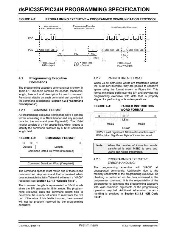
After the programming executive has processed the
command, it brings PGD low for 15
渭sec
to indicate to
the programmer that the response is available to be
clocked out. The programmer can begin to clock out
the response 23
渭sec
after PGD is brought low and it
must provide the necessary amount of clock pulses to
receive the entire response from the programming
executive.
After the entire response is clocked out, the program-
mer should terminate the clock on PGC until it is time
to send another command to the programming
executive. This protocol is shown in Figure 4-2.
4.1.2
SPI RATE
4.1.1
COMMUNICATION INTERFACE
AND PROTOCOL
In Enhanced ICSP mode, the dsPIC33F/PIC24H family
devices operate from the Fast Internal RC oscillator,
which has a nominal frequency of 7.3728 MHz. This
oscillator frequency yields an effective system clock
frequency of 1.8432 MHz. To ensure that the program-
mer does not clock too fast, it is recommended that a
7.35 MHz clock be provided by the programmer.
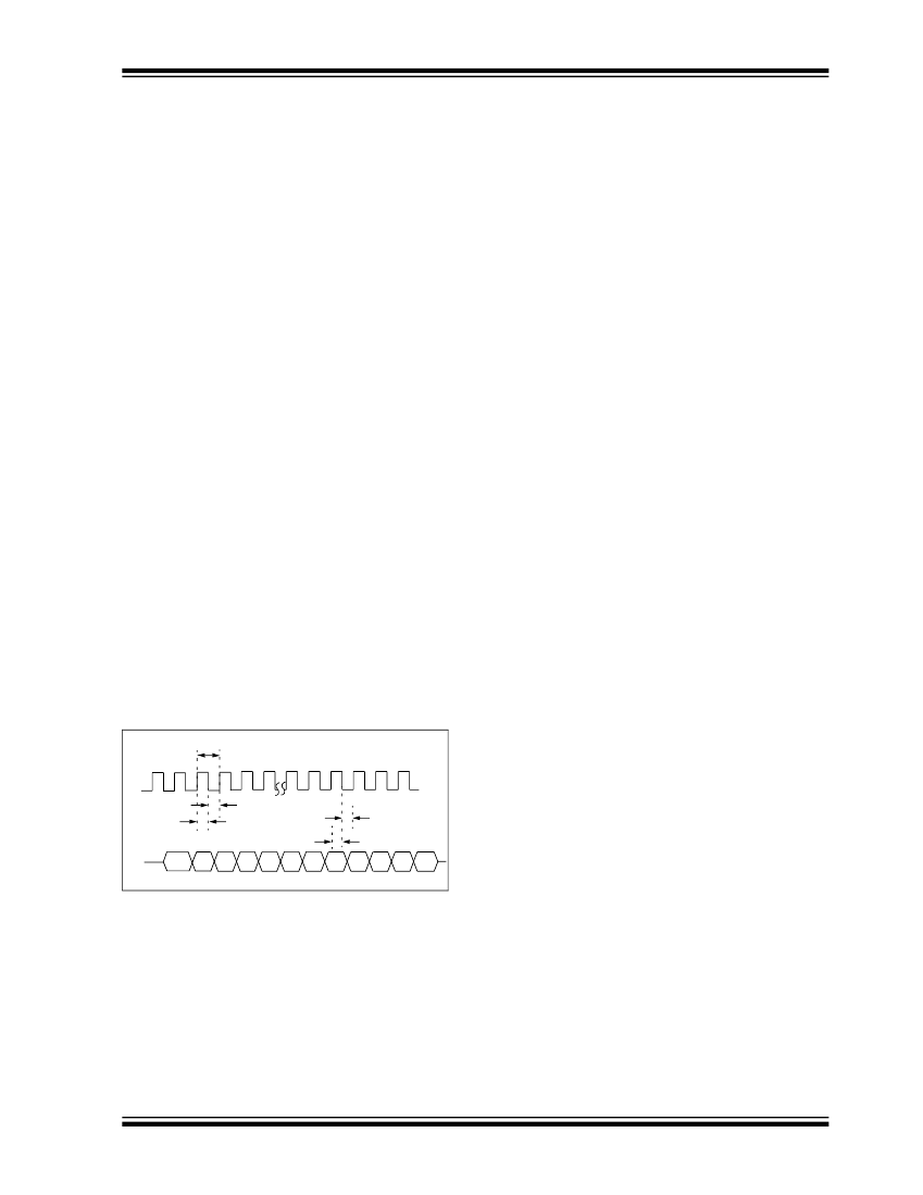
The ICSP/Enhanced ICSP interface is a 2 wire SPI
implemented using the PGC and PGD pins. The PGC
pin is used as a clock input pin and the clock source
must be provided by the programmer. The PGD pin is
used for sending command data to and receiving
response data from the programming executive. All
serial data is transmitted on the falling edge of PGC
and latched on the rising edge of PGC. All data trans-
missions are sent to the Most Significant bit (MSb) first
using 16-bit mode (see Figure 4-1).
4.1.3
TIME OUTS
The programming executive uses no Watchdog or time
out for transmitting responses to the programmer. If the
programmer does not follow the flow control
mechanism using PGC as described in
Section 4.1.1
鈥淐ommunication Interface and Protocol鈥?
it is
possible that the programming executive will behave
unexpectedly while trying to send a response to the
programmer. Since the programming executive has no
time out, it is imperative that the programmer correctly
follow the described communication protocol.
As a safety measure, the programmer should use the
command time outs identified in Table 4-1. If the
command time out expires, the programmer should
reset the programming executive and start
programming the device again.
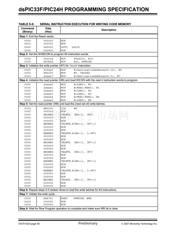
FIGURE 4-1:
PROGRAMMING
EXECUTIVE SERIAL
TIMING
4
5
6
11
12
13 14
15 16
P1
1
PGC
P1A
P1B
P2
PGD
MSb 14
13
12
11
...
5
4
3
2
1 LSb
P3
2
3
Since a 2 wire SPI is used, and data transmissions are
bidirectional, a simple protocol is used to control the
direction of PGD. When the programmer completes a
command transmission, it releases the PGD line and
allows the programming executive to drive this line
high. The programming executive keeps the PGD line
high to indicate that it is processing the command.
漏
2007 Microchip Technology Inc.
Preliminary
DS70152D-page 47


 1
1
 2
2
 3
3
 4
4
 5
5
 6
6
 7
7
 8
8
 9
9
 10
10
 11
11
 12
12
 13
13
 14
14
 15
15
 16
16
 17
17
 18
18
 19
19
 20
20
 21
21
 22
22
 23
23
 24
24
 25
25
 26
26
 27
27
 28
28
 29
29
 30
30
 31
31
 32
32
 33
33
 34
34
 35
35
 36
36
 37
37
 38
38
 39
39
 40
40
 41
41
 42
42
 43
43
 44
44
 45
45
 46
46
 47
47
 48
48
 49
49
 50
50
 51
51
 52
52
 53
53
 54
54
 55
55
 56
56
 57
57
 58
58
 59
59
 60
60
 61
61
 62
62
 63
63
 64
64
 65
65
 66
66
 67
67
 68
68
 69
69
 70
70
 71
71
 72
72
 73
73
 74
74
 75
75
 76
76
 77
77
 78
78
 79
79
 80
80
