鈥?/div>
User Unit ID Byte 0
User Unit ID Byte 1
User Unit ID Byte 2
User Unit ID Byte 3
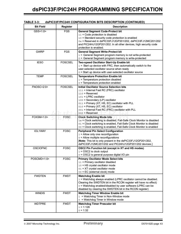
FNOSC<2:0>
OSCIOFNC
0xF80006 FOSCSEL
POSCMD<1:0>
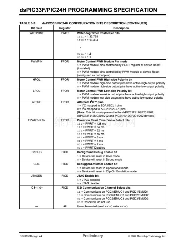
WDTPOST<3:0>
FPWRT<2:0>
ICS<1:0>
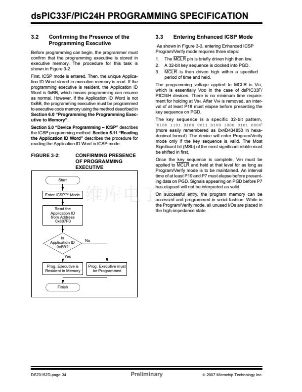
On the dsPIC33F General Purpose Family devices (dsPIC33FJXXXGPXXX) and PIC24H devices, these
bits are reserved (read as 鈥?鈥?and must be programmed as 鈥?鈥?.
These bits are only present in the dsPIC33FJ12GP201/202, dsPIC33FJ12MC201/202 and
PIC24HJ12GP201/202 devices. In all other devices, they are unimplemented (read as 鈥?鈥?.
In the dsPIC33FJ12GP201/202, dsPIC33FJ12MC201/202 and PIC24HJ12GP201/202 devices, these bits
are reserved (read as 鈥?鈥?and must be programmed as 鈥?鈥?.
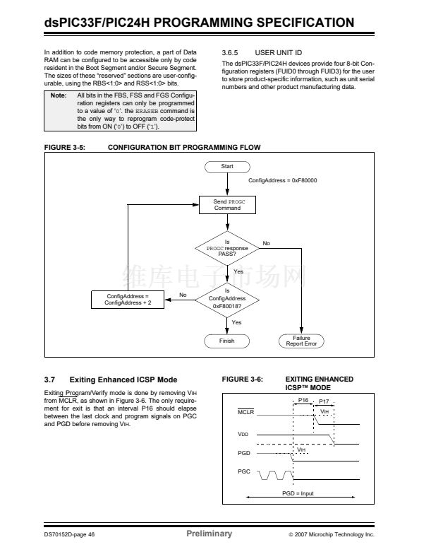
3.6.2
PROGRAMMING METHODOLOGY
3.6.4
Configuration bits may be programmed a single byte at
a time using the
PROGC
command. This command
specifies the configuration data and Configuration
register address. When Configuration bits are
programmed, any unimplemented bits must be
programmed with a 鈥?鈥?and any reserved bits must be
programmed with a 鈥?鈥?
Twelve
PROGC
commands are required to program all
the Configuration bits. A flowchart for Configuration bit
programming is shown in Figure 3-5.
Note:
If the General Code Segment Code-
Protect bit (GCP) is programmed to 鈥?鈥?
code memory is code-protected and
can not be read. Code memory must
be verified before enabling read protec-
tion. See
Section 3.6.4 鈥淐odeGuard
Security Configuration Bits鈥?/span>
for more
information about code-protect Configura-
tion bits.
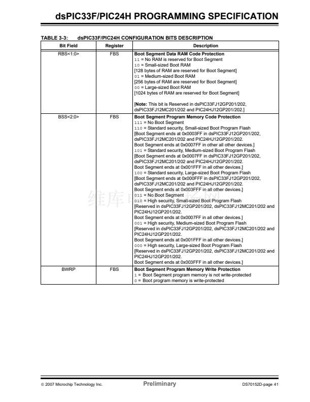
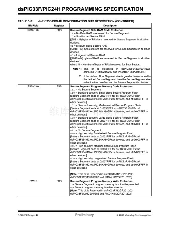
CODEGUARD SECURITY
CONFIGURATION BITS
The FBS, FSS and FGS Configuration registers are
special Configuration registers that control the size and
level of code protection for the Boot Segment, Secure
Segment and General Segment, respectively. For each
segment, two main forms of code protection are
provided. One form prevents code memory from being
written (write protection), while the other prevents code
memory from being read (read protection).
BWRP, SWRP and GWRP bits control write protection
and BSS<2:0>, SSS<2:0> and GSS<1:0> bits controls
read protection. The Chip Erase
ERASEB
command
sets all the code protection bits to 鈥?鈥? which allows the
device to be programmed.
When write protection is enabled, any programming
operation to code memory will fail. When read protec-
tion is enabled, any read from code memory will cause
a 鈥?x0鈥?to be read, regardless of the actual contents of
code memory. Since the programming executive
always verifies what it programs, attempting to program
code memory with read protection enabled will also
result in failure.
It is imperative that all code protection bits are 鈥?鈥?while
the device is being programmed and verified. Only after
the device is programmed and verified should any of
the above bits be programmed to 鈥?鈥?
3.6.3
PROGRAMMING VERIFICATION
After the Configuration bits are programmed, the
contents of memory should be verified to ensure that
the programming was successful. Verification requires
the Configuration bits to be read back and compared
against the copy held in the programmer鈥檚 buffer. The
READC
command reads back the programmed
Configuration bits and verifies that the programming
was successful.
Any unimplemented Configuration bits are read-only
and read as 鈥?鈥? The reserved bits are read-only and
read as 鈥?鈥?
漏
2007 Microchip Technology Inc.
Preliminary
DS70152D-page 45


 1
1
 2
2
 3
3
 4
4
 5
5
 6
6
 7
7
 8
8
 9
9
 10
10
 11
11
 12
12
 13
13
 14
14
 15
15
 16
16
 17
17
 18
18
 19
19
 20
20
 21
21
 22
22
 23
23
 24
24
 25
25
 26
26
 27
27
 28
28
 29
29
 30
30
 31
31
 32
32
 33
33
 34
34
 35
35
 36
36
 37
37
 38
38
 39
39
 40
40
 41
41
 42
42
 43
43
 44
44
 45
45
 46
46
 47
47
 48
48
 49
49
 50
50
 51
51
 52
52
 53
53
 54
54
 55
55
 56
56
 57
57
 58
58
 59
59
 60
60
 61
61
 62
62
 63
63
 64
64
 65
65
 66
66
 67
67
 68
68
 69
69
 70
70
 71
71
 72
72
 73
73
 74
74
 75
75
 76
76
 77
77
 78
78
 79
79
 80
80
